Passion for Power Solutions

Industrial I Components
1200V SiC Schottky barrier diodes to reduce power loss
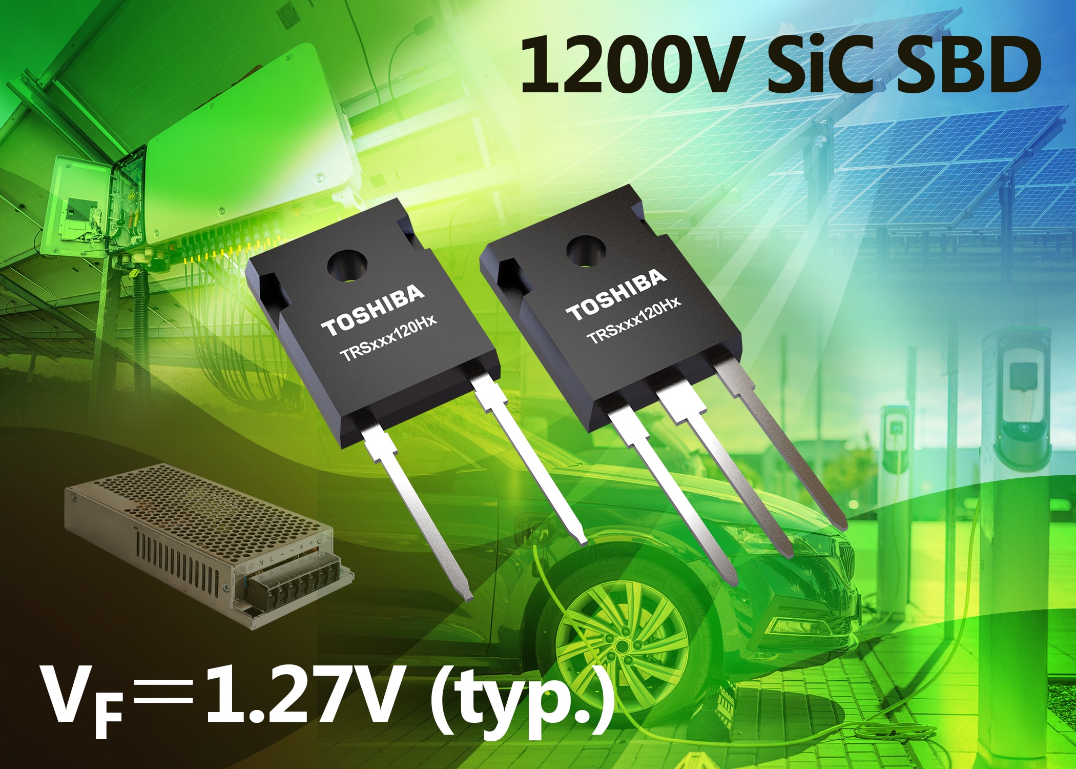
Devices achieve typical low forward voltage of 1.27V
The ten 1200V Schottky barrier diodes (SBDs) of the TRSxxx120Hx series comprise five products housed in TO-247-2L packages and five in TO-247 packages. The devices helps designers improve the efficiency of industrial equipment, including photovoltaic (PV) inverters, electric vehicle (EV) charging stations, and switching power supplies. By implementing an enhanced junction barrier Schottky (JBS) structure, the TRSxxx120Hx series allows a very low forward voltage (VF) of just 1.27V (typ.). Combined with the lower capacitive charge and leakage current, the products can support the improvment of system efficiency and simplify thermal design. Read the full press release
| Features | Advantages | Benefits |
|---|---|---|
|
|
|
3rd generation Silicon Carbide(SiC) MOSFETs
-mosfets_features_1_en.png)
Introduction of 650V and 1200V voltage products
In common with 2nd generations, Toshiba's newest generation of MOSFETs include a built-in SiC Schottky Barrier Diode (SBD) with a low forward voltage (VF) of -1.35V (typ.), placed in parallel with the PN diode in the SiC MOSFETs, to suppress fluctuation in RDS(on) thereby enhancing reliability. Furthermore, Toshiba’s advanced SiC process[1] has greatly improved our on-resistance per unit area RonA, and the performance index Ron*Qgd, which indicates switching characteristics, compared to 2nd generation products. Also, it has easy to design gate drive circuit, and you can prevent malfunctions due to switching noise.
Applications:
Toshiba's 3rd generation SiC MOSFETs provides lower power consumption and supports higher power density for applications such as switching power supplies (servers for data centers, communication equipment), uninterruptible power supplies (UPS), PV inverters, EV charging stations etc.
650V SiC Schottky Barrier Diodes
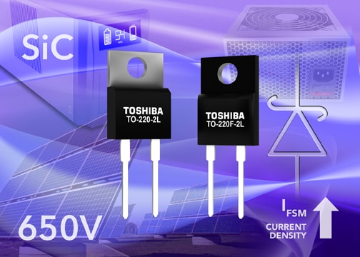
2nd Generation of devices offer higher current density
With densities up to 50% higher than the first generation, Toshiba's devices and can handle significantly higher forward surge currents. The use of SiC semiconductors helps designers to improve efficiency, reduce heat dissipation and save space in high-speed power switching designs. SiC power devices also offer stable operation over a wider temperature range than silicon alternatives – even at high voltages and currents.
Key product:
Check for more:

Applications:
- Power factor correction (PFC) at power supply
- Photovoltaic inverters
- Uninterruptible power supplies (UPS)
| Features | Advantages | Benefits |
|---|---|---|
|
|
|
650V SiC Schottky Barrier Diode Line-up
| VRRM (V) | IF(DC) (A) | TO-220F-2L | TO-220-2L | TO-247 |
|---|---|---|---|---|
| 650 | 2 | TRS2E65F | ||
| 3 | TRS3E65F | |||
| 4 | TRS4A65F |
TRS4E65F | ||
| 6 | TRS6A65F |
TRS6E65F | ||
| 8 | TRS8A65F |
TRS8E65F | ||
| 10 | TRS10A65F |
TRS10E65F | ||
| 12 | TRS12A65F |
TRS12E65F | TRS12N65FB | |
| 16 | TRS16N65FB | |||
| 20 | TRS20N65FB | |||
| 24 | TRS24N65FB |
High Voltage 650V Series Superjunction MOSFETs | DTMOSVI

More efficient switching power supplies
The 650V-rated N-channel power MOSFETs strengthen Toshiba's latest DTMOSVI series with highly appealing performance parameters. These devices offer designers a 40% reduction in terms of their drain-source on-resistance x gate-drain charge (QGD) figure of merit (FoM) when compared to the previous DTMOS generation. As a consequence, they can raise the efficiency of switch-mode power supplies thereby enabling a substantial decrease in switching losses, compared to the previous generation
Key product:
High Voltage MOSFETS - DTMOSVI Overview
Check for more:
Applications:
- Switching power supplies in industrial equipment, data centers and power conditioners of photovoltaic generators
| Features | Advantages | Benefits |
|---|---|---|
|
|
|
High Voltage 650V Series Superjunction MOSFETs Line-up | DTMOS VI
| Rds(ON) maxΩ) |
DFN8x8 |
TO-220SIS |
TO-247 | TO-247-4L | TOLL | Qg (nC) Typ. |
Ciss (VDS=300V) (pF) Typ. |
|---|---|---|---|---|---|---|---|
| 0.19 / 0.21 | TK210V65Z | TK190A65Z | TK190U65Z | 25 | 1370 | ||
| 0.155 / 0.17 | TK170V65Z | TK155A65Z | TK155U65Z | 29 | 1635 | ||
| 0.11 / 0.125 | TK125V65Z |
TK110A65Z | TK110N65Z | TK110Z65Z | 40 | 2250 | |
| 0.090 / 0.099 | TK099V65Z | TK090A65Z | TK090N65Z | TK090Z65Z | 47 | 2780 | |
| 0.065 | TK065N65Z | TK065Z65Z | TK065U65Z | 62 | 3650 | ||
| 0.040 | TK040N65Z | TK040Z65Z | 105 | 6250 |
Low-spike-type 40V N-channel Power MOSFET | U-MOS IX-H
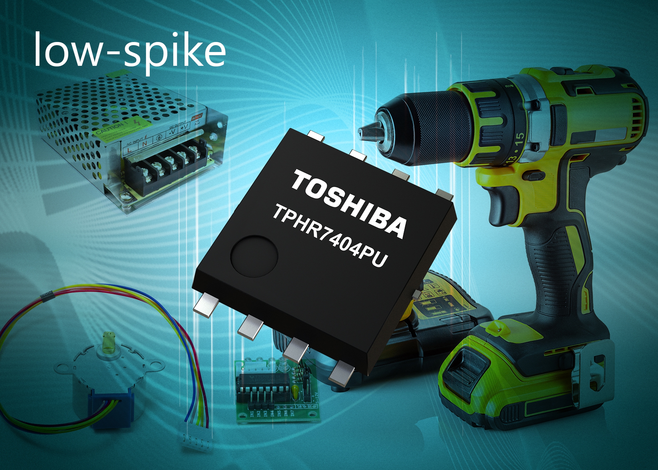
Reduction of EMI in switching power supply applications
Utilizing excellent high-speed performance, TPHR7404PU`s small 5 x 6mm SOP Advance package and extraordinary low 0.71°C/W channel-to-case thermal resistance makes the device suitable for efficiency-focused, compact power solutions. Low spike performance MOSFETs will simplify designers job and help to avoid EMI issue.
Key product:
Applications:
- Power tools
- DC/DC converter
- Synchronous rectifier
| Features | Advantages | Benefits |
|---|---|---|
|
|
|
80V Series N-channel Power MOSFETs | U-MOS X-H
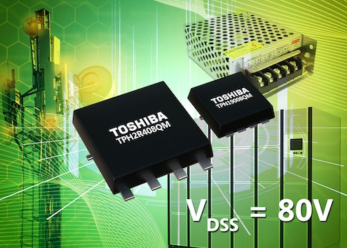
Devices can significantly enhance power supply efficiency
TPH2R408QM and TPN19008QM are based upon Toshiba's latest generation U-MOSX-H process that exhibit a reduction of around 40% in drain-source on-resistance (Rds(ON)) compared to corresponding 80V products in earlier processes.
Applications:
- Telecom Power supply
- Industrial Power supply synchronous rectification at 24~28V output Voltage
- Motor drive Power stage at 36V power Tool
| Features | Advantages | Benefits |
|---|---|---|
|
|
|
80V Series N-channel Power MOSFETs Line-up | U-MOS X-H
| Part Number | Rds (on) | Package size |
Package name |
|---|---|---|---|
| TPH3R008QM | 3 mΩ | 4.9 x 6.1 mm | SOP Advance (N) |
| TPH4R008QM | 4 mΩ | 4.9 x 6.1 mm | SOP Advance (N) |
| TPH6R008QM | 6 mΩ | 4.9×6.1 mm | SOP Advance (N) |
| TPN12008QM | 12 mΩ | 3 x 3 mm | TSON Advance |
| TPN19008QM | 9 mΩ | 3 x 3 mm | TSON Advance |
| TPN8R408QM | 8,4 mΩ | 3 x 3 mm | TSON Advance |
| TPH8R808QM | 8.8 mΩ | 4.9×6.1 mm | SOP Advance (N) |
80V Gate Driver ICs for Three-Phase Brushless DC Motors
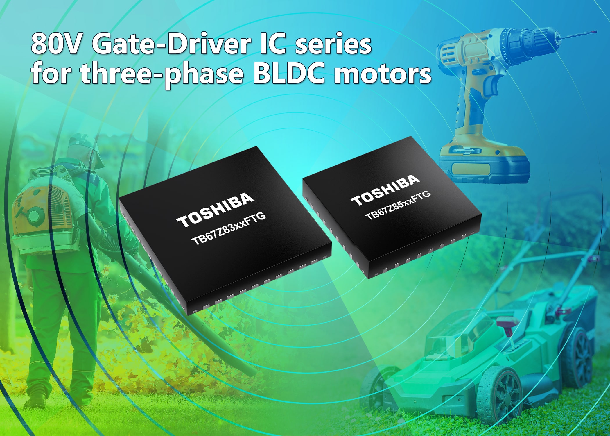
In combination with an MCU and MOSFETs, a complete system solution is possible
The Gate Driver IC series for three-phase brushless DC motors is designed for industrial and consumer applications. The TB67Z83xxFTG (with 3.3V regulator output) and TB67Z85xxFTG (with 5.0V regulator output) series, both comprising four devices, can be combined with a motor control microcontroller and MOSFETs to create a complete system for a wide range of applications including pumps, fans, blowers, cordless power tools, gardening tools and cleaners. Featuring built-in circuits, the new products can drive three phases of high-side and low-side N-channel MOSFETs., with a drive current that can be set from 10mA to 1A (peak) for source current and from 20mA to 2A (peak) for sink current – though operating conditions, such as ambient temperature and power supply voltage, may limit the actual useful drive current. All devices support a supply voltage (VM) operating range from 8V to 75V. This selection of different voltage and current combinations covers a wide range of applications.
Applications:
- Fans
- Pumps
- Cordless power-, cleaner-, gardening tools
- Robots
| Features | Advantages | Benefits |
|---|---|---|
|
|
|
Improved Power Efficiency by using 150V N-channel MOSFET

New devices are based on Toshiba latest low voltage generation U-MOS X-H process
TPH9R00CQH and TPH9R00CQ5MOSFET have a very low drain-source on-resistance RDS(ON) of just 9.0mΩ (max. @ VGS=10V). This represents a reduction of approximately 42% when compared to the existing 150V product (TPH1500CNH) that is based upon the current generation U-MOSVIII-H process. The new components offers two surface mount (SMD) package options – SOP Advance (5.0mm x 6.0mm) and SOP Advance(N) (4.9mm x 6.1mm) which can be selected to meet the needs of any application.
Applications:
High efficiency DC-DC convertor
Switching voltage regulator
Motor drives
| Features | Advantages | Benefits |
|---|---|---|
|
|
|
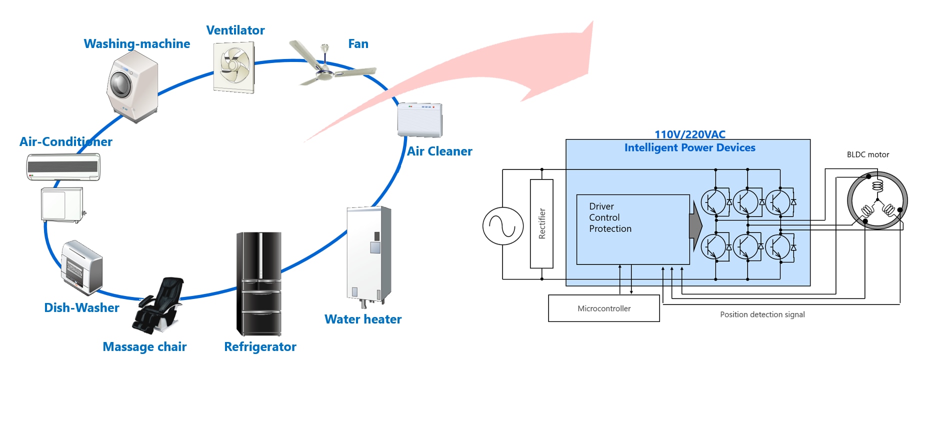
Compact intelligent power device (IPD) with 600V rating
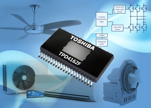
Efficient operation reduces power consumption of motor equipment
The TPD4162F is suitable for any applications with input signals in the range up to 220V AC. It contains a PWM circuit, 3-phase decoder, level shifting high-side driver and low side driver with embedded IGBTs and FRDs. Multiple protection features include current limit, over current protection (OCP), thermal shutdown and undervoltage lockout (UVLO).
Key products:
Applications:
- Air conditioners
- Air cleaners
- Pumps
| Features | Advantages | Benefits |
|---|---|---|
|
|
|
TPD4162F Block Diagram
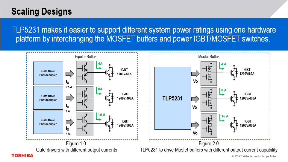
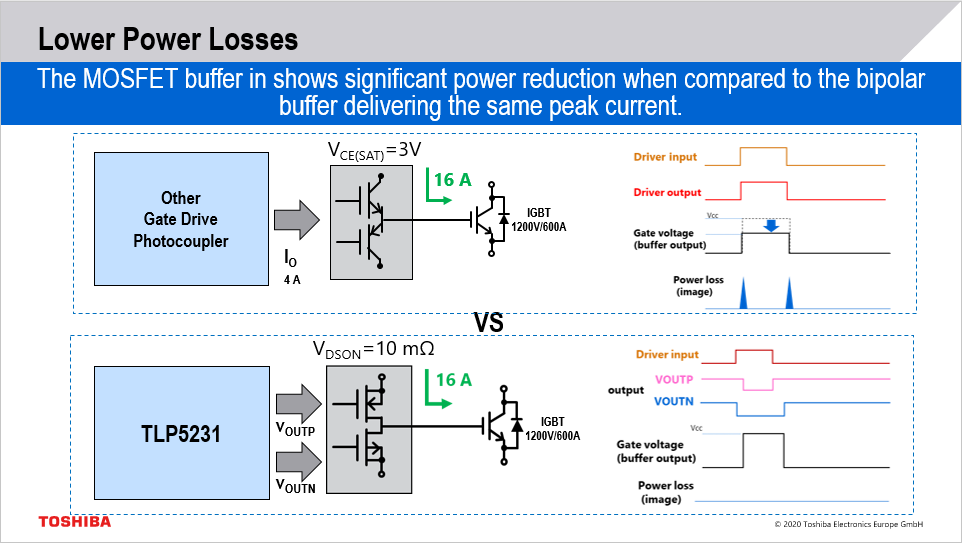
Smart Gatedriver Family to control (SiC) MOSFETs and IGBTs
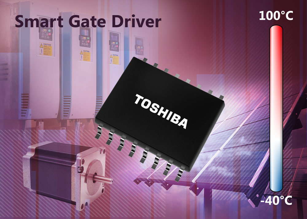
Sophisticated devices incorporate numerous protection functions
Controling IGBTs as well (SiC) MOSFETs these smart gate drivers are suitable fora wide range of applications including inverters, AC servo drives, photovoltaic (PV) inverters and uninterruptible power supplies (UPSs). They incorporate protection functions such as MOSFET and IGBT desaturation detection, active Miller clamp, U(VLO) and FAULT output, eliminating the need for several external circuits. This reduces system costs for fault detection and protection and saves space on the board and minimizes design effort. Drive strengths from +/-2.5A up to +/-4A can be supported at a wide output voltage range from 15V to 30V with low propagation delay.
Applications
- Industrial inverters
- Uninterruptible power supplies (UPS)
- Power conditioners for solar energy
- Power conditioners for motor controls
Check for more:
| Features | Advantages | Benefits |
|---|---|---|
|
|
|
Smart Gate Driver Graphics
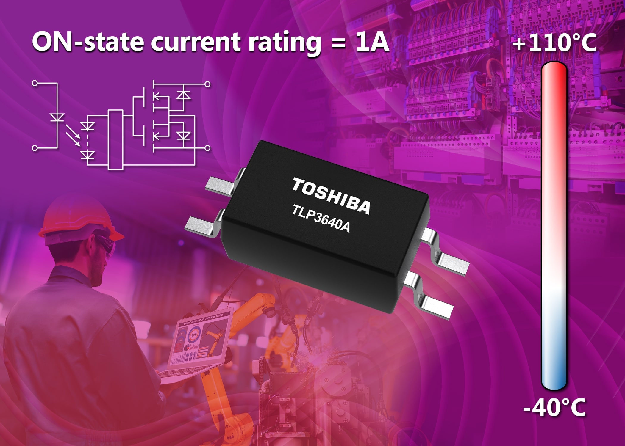
Compact Photorelay with High ON-State Current
Long life, low power consumption and silent operation
The silent, normally open TLP3640A replaces conventional 1-Form-A mechanical relays to improve system reliability and reduce power consumption. Housed in the 4-pin SO4 package measuring only 2.6mm x 7mm (typ.), the mounting area is reduced by 70% compared to mechanical relays and 30% compared to Toshiba’s TLP3122A device, contributing to application downsizing and reducing PCB cost. The new photorelay is fabricated using Toshiba’s proprietary chip-on-chip technology (3D integration technology with vertical chip stacking) to deliver an off-state output terminal voltage (VOFF) of 60V (min.), a constant on-state current (ION) of 1A (max.), and an on-state pulsed current (IONP) of up to 3A. Read full press release
| Features | Advantages | Benefits |
|---|---|---|
|
|
|
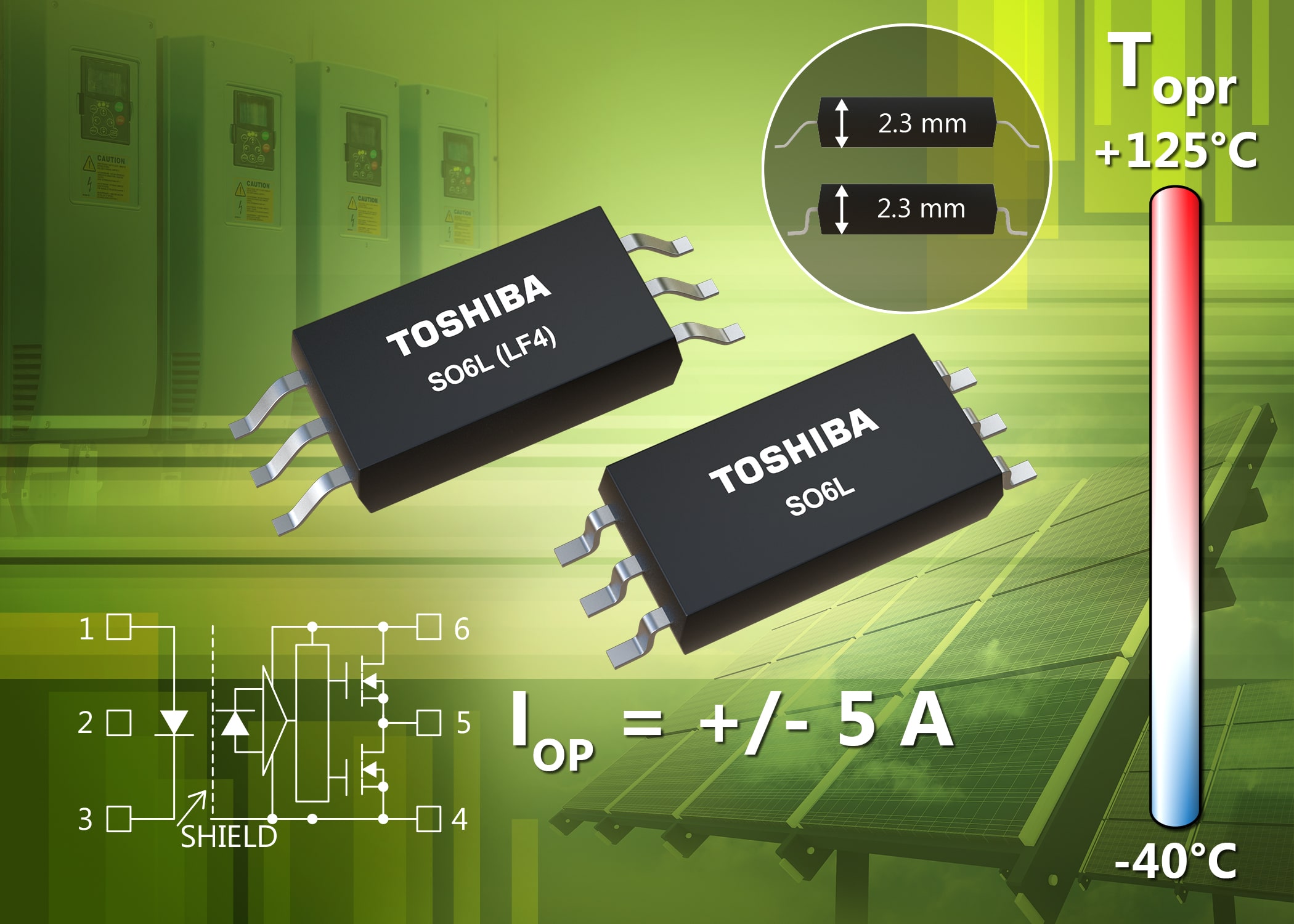
New High Peak Output Current Photocouplers
Ultra-thin SO6L package offers easy upgrade path to reduce height in designs
The use of the new photocouplers TLP5702H and TLP5705H can help simplifying designs, reducing part count and enabling miniaturisation. Whilst TLP5705H is Toshiba’s first product to deliver a peak output current rating of ±5.0A, the TLP5702H has a peak output current rating of ±2.5A. With a footprint of just 10.0mm x 3.84mm the ultra-thin SO6L package can be mounted on the PCB land pattern of a conventional SDIP6 package, facilitating an easy upgrade path for Toshiba’s current photocouplers, such as the TLP700H. The rugged devices are ideally suited to applications in industrial equipment.
Applications:
- Industrial Inverters
- PV Inverter
- AC Servo Drives, UPS
| Features | Advantages | Benefits |
|---|---|---|
|
|
|
High-Speed Photo-IC Coupler

10Mbps logic output photocoupler for PLCs
The new TLP2363 is rated for a wide operating temperature range (-40 to +105°C). The threshold input current (IFHL) is specified with min. 0.3mA and max. 2.4mA thereby ensuring conformance to the digital input standard IEC 61131-2 type 1. Uniquely for this type of device, all that is required to complete the design is a bridge diode and a suitable resistor for current control. The short propagation delay of just 80ns is ideal for use with high-speed systems.
Key product:
Applications:
- 24V digital input programmable logic controller (PLC)
- Measurement and control equipment
| Features | Advantages | Benefits |
|---|---|---|
|
|
|
High Speed IC Coupler Circuit Diagram

- Compliance with IEC61131-2 standard for PLC digital input modules (type 1) by combination with 2 resistors
- Guaranteed minimum and maximum threshold input current at whole range of operating temperature
- High immunity to slow input for both LED side and detector side to contribute to the gradual shut-down/start up test for PLC
Isolators/Solid State Relays - Photorelays
Improve safety, cut power consumption and reduce the size of end products
Photorelays are a type of photocoupler consisting of an LED optically coupled with a MOSFET. They offer many advantages over mechanical relays such as long operational life, low-current drive and fast response. Widely used for contact switching in various industrial applications, Toshiba photorelays provide low RON, low COFF devices in various packages featuring high current and high off-state voltage.
Applications:
- Factory automation
- Programmable Logic Controllers
- Security systems
- Measurement equipment
- Heating ventilation and air conditioning
- Battery management systems
- Automatic test equipment
- Smart meters
| Features | Advantages | Benefits |
|---|---|---|
|
|
|
Industrial I Solutions
Sic Cube for EV Charging
Watch the explanation of our modular SiC Cube concept for an EV charger reference design. You can find out more about the benefits of Toshiba’s SiC MOSFETs in our SiC Snack flyers:
- Switching Capabilities
- The RDS(ON) x Qgd figure of merit (FoM)
- Suppressing Body Diode Conduction Effects
- Wide VGSS ratings
- Advanced packaging with Kelvin source pin
Additional information about our line-up, you find on our and dedicated webpage.
Brushed Motor Driver - Lowest standby power consumption
Ultra-low standby current consumption
- Only 1µA standby current
- Wide operating voltage range down to 4.5V
- Enables multi-product sourcing strategies due to industry standard package and pinout
Key products: TB67H450AFNG TB67H451AFNG
MIKROE ClickboardTM TB67H450AFNG
MIKROE ClickboardTM TB67H451AFNG
Check for more: Download TB67H450FNG press release (Predecessor)
| Features | Advantages | Benefits |
|---|---|---|
|
|
|
Brushless DC Motor Control
Constant rotational speed via closed-loop speed control
- Fast regulation of speed fluctuations caused by changes in power supply voltage and torque load
- No external MCU required due to embedded non-volatile memory
- No speed control software development required
- Intelligent Phase Control detects the motor current phase and feeds back the information for auto lead angle control (see video)
Key products:
| Features | Advantages | Benefits |
|---|---|---|
|
|
|
Stepper Motor Control
Precice and efficient control of linear motion systems
- High accuracy and low noise by 128 micro step mode
- High flexibility by SPI control, 1024 mico steps option
- Highest efficiency by low RDS(ON), 0.48 Ohm and 0.1uA standby current
Key product:
| Features | Advantages | Benefits |
|---|---|---|
|
|
|
*1) Active Gain Control optimizes the drive current to suit the required torque. It´s a Toshiba technology that prevents stalls and realizes power savings.
*2) Advanced Dynamic Mixed Decay automatically optimizes switching control of fast decay and slow decay modes to secure high speed rotation. It´s a Toshiba original mixed decay technology.
Videos about Active Gain Control
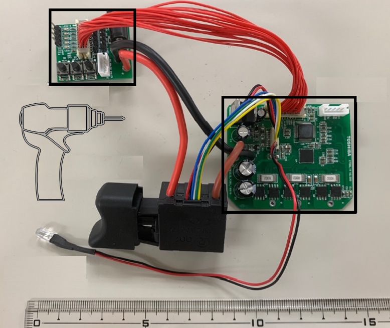
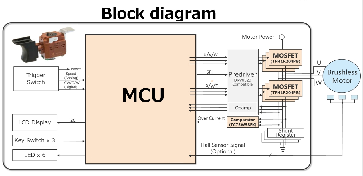
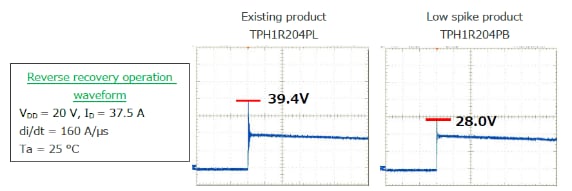
Cordless Power Tool Reference Design
Compact, efficient and flexible control for Brushless DC (BLDC) motor based power tools
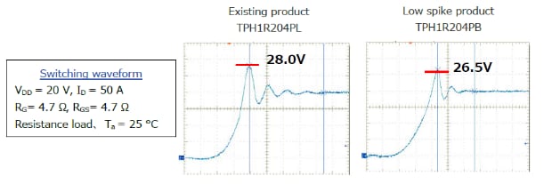
The reference design combines Toshiba’s highly efficient low-voltage MOSFET devices with Toshiba’s dedicated motor control MCU and thus provides a very compact but flexible platform for the control and drive of BLDC motors in power tools. The Motor current is generated by a 3-phase inverter with 200W output power stage using the Toshiba TPH1R204PB low-voltage MOSFET. This device features industry-leading RDS(ON) in a 5×6mm SOP Advanced package and provides low spike generation helping to prevent EMI effects.
Main PCB
• Compact form factor (60 x 50 mm)
• 3-phase inverter, 200W output stage
• Speed control switch
• Pilot lamp
* sofware currently under development
| Features | Advantages | Benefits |
|---|---|---|
|
|
|
* optional support
Board picture & block diagram

* Optional support
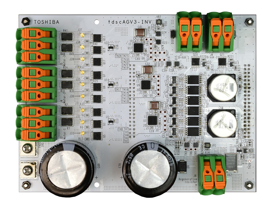
Automatic Guided Vehicle Reference Model (AGV)
Inverter for 3-phase motor drive and MCU for BLDC servo motor control
- Inverter for three 3-phase brushless DC motors, up to 750W each
- AGV moving with three omni wheels of 203mm diameter
- Line tracing through infrared sensor system
Key products:
| Features | Advantages | Benefits |
|---|---|---|
|
|
|
Picture of reference board
Servo Drive Reference Model for Multi-Channel Motor Control
Robot ARM as demo system
- Robot arm movement by single MCU controlling 3 motors
- Inverter drives 3-phase BLDC motors, 200W power stage
Key products:
TMPM4KNFYADFG Motor MCU (160MHz)
Low-Voltage TPW3R70APL MOSFET | U-MOS IX
M4K Motor Control MCU Series
| Features | Advantages | Benefits |
|---|---|---|
|
|
|
Automotive I Components
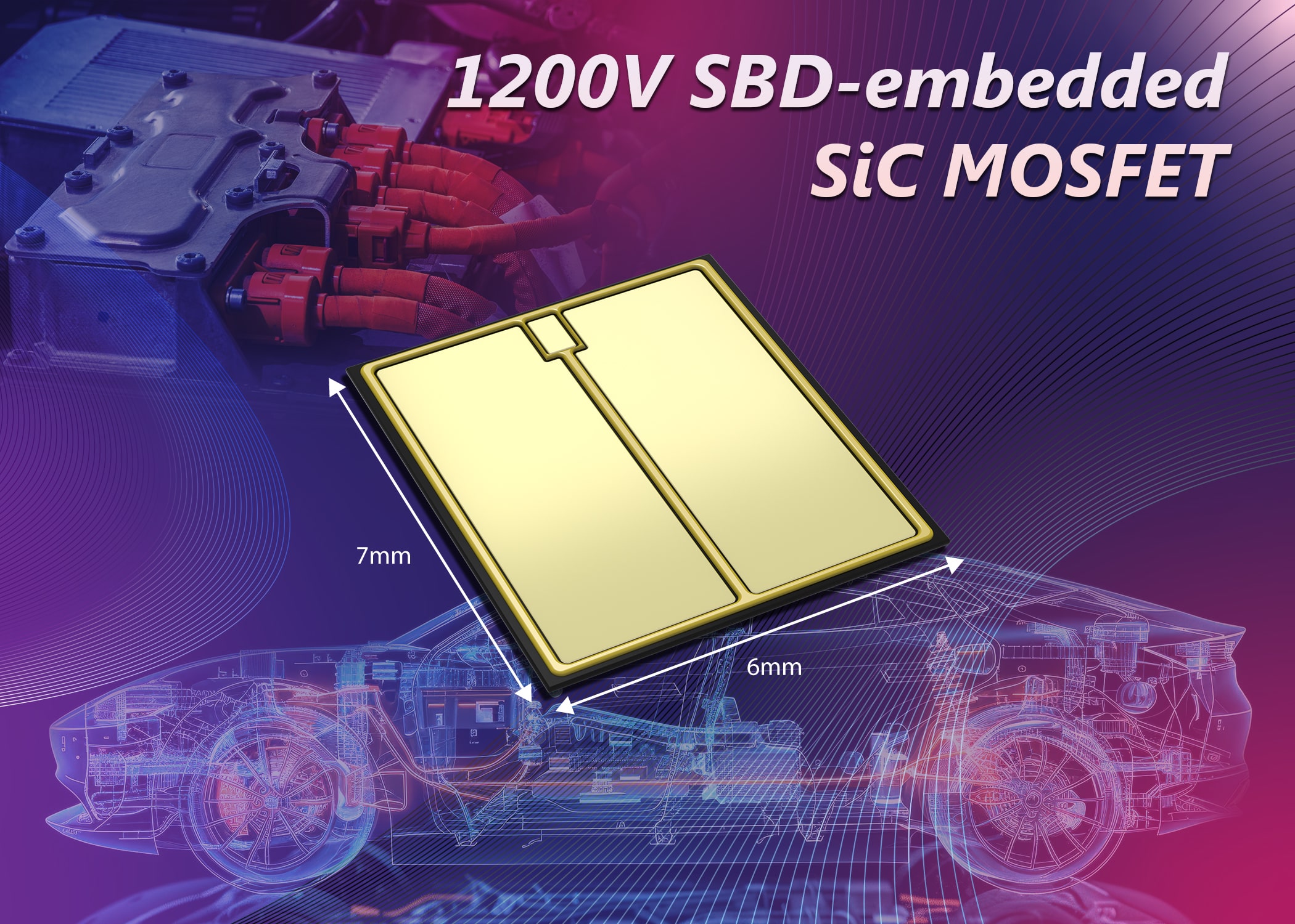
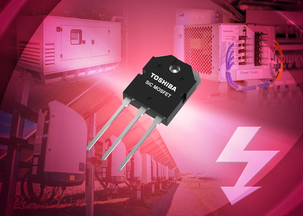
Bare die format of 1200V SiC MOSFETs available
Devices offer low resistance and high reliability for automotive traction inverter
Toshiba has developed new 1200V silicon carbide (SiC) MOSFETs with low on-resistance (RDS(ON)) and high levels of reliability. The devices are particularly suited to applications within automotive traction inverters. They are now available and shipping as early test samples in bare die format – allowing customers to customise them to meet the needs of their applications.
The new X5M007E120 uses a manufacturing process that reduces on-resistance per unit area by up to 30%. Unlike existing methods that utilise a striped-pattern construction, the new devices arrange the embedded Schottky barrier diodes (SBDs) in a check-pattern to achieve lower on-resistance.
| Features | Advantages | Benefits |
|---|---|---|
|
|
|
Compact N-channel MOSFETs with 3.3x3.6mm package

Package that contributes to the miniaturization of ECU
Highly efficient and compact devices in TSON Advance (WF) package for the first time, which ensure that board utilization is kept to a minimum.
Key products:
Check for more:
Automotive MOSFETs Product Overview
Applications:
- Automotive equipment applications such as switching regulators, DC-DC converters and motor drivers.
| Features | Advantages | Benefits |
|---|---|---|
|
|
|
100V process technology MOSFETs
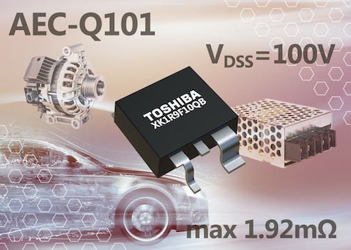
New device is the first to be produced in Toshiba’s new U-MOS X-H series
Withstanding a drain-source voltage (VDSS) of 100V the new XK1R9F10QB is rated for a continuous drain current (ID) of 160A, or 480A if pulsed (IDP) and can be operated with a channel temperature of 175°C.
Key products:
Check for more:
Automotive MOSFETs Product Overview
Applications:
- Automotive equipment applications such as load switches, switching power supplies and driving of motors
| Features | Advantages | Benefits |
|---|---|---|
|
|
|
100V N-channel MOSFETs with 5x6mm package
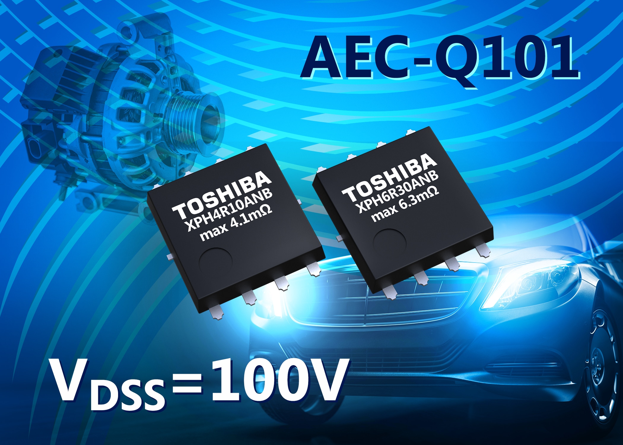
Highly efficient devices in SOP Advance (WF) package for the first time
Designed specifically for modern 48V system applications, the devices are suited to use in boost converters for integrated starter generators (ISG) and LED headlights as well as motor drives, switching regulators and load switches. They are available in a small surface mount SOP Advance wettable flanks package.
Key products:
XPH4R10ANB Power MOSFET (N-ch single 60V<VDSS≤150V)
XPH6R30ANB Power MOSFET (N-ch single 60V<VDSS≤150V)
Applications:
- Automotive equipment
- Power supply (DC/DC converter) and LED headlights, etc. (motor drives, switching regulators and load switches)
| Features | Advantages | Benefits |
|---|---|---|
|
|
|
Low Voltage MOSFET with smaller packages
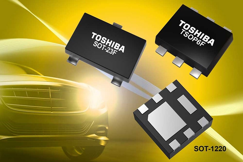
Higher density and less power losses
These devices meet the increasing need of the industry for smaller, efficient MOSFETs. They are part of Toshiba`s smaller package portfolio which offer a wide choice of package sizes ranging from 1x1 mm-class ultra-small packages to 3x3 mm, which contributes to miniaturization of sets by reducing the mounting area and increasing power density. By combining latest wafer processes with low-resistance packaging technologies, an industry-leading level of low on-resistance MOSFET is achieved.
Applications:
- Motor drives
- DC-DC converter
- Switching regulator for automotive
| Features | Advantages | Benefits |
|---|---|---|
|
|
|
10A H-Bridge Drivers

Configurable in 2 x 5A Dual-Channel Mode
Qualified according to AEC-Q100 Grade 1, TB9053* and TB9054* (TB9053/54FTG Datasheet) integrate two separated 5A H-bridge channels to directly drive DC brushed motors. 10A 1-channel motor drive is possible when both channels are configured to operate in parallel. Motors can be controlled in real-time either by conventional PWM signals or by SPI, daisy-chain mode is also supported. The SPI interface is also used for advanced diagnosis as well as device parametrization. Various failure detection mechanisms ensure a safe system operation.
* Under development; Samples available on request
Applications
• ETC (Engine Throttle Control)
• EGR (Exhaust Gas Recirculation)
• Power mirror folding
• Lid actuator for rear-view camera or OBC socket
• Grill shutter control
• Seat adjustment
• Power door opening & closing
• Shift-by-wire actuators
• Small fans
| Features | Advantages | Benefits |
|---|---|---|
|
|
|
Automotive BLDC pre-driver IC supporting ASIL-D
Device can address a broad range of safety-critical in-vehicle applications
TB9083FTG is intended for use with the numerous brushless DC (BLDC) motors being featured in modern automotive designs and is designed in accordance with ISO 26262 (2nd edition) and supports up to ASIL-D level functional safety. Among its key applications are electric power steering systems (EPS), electric braking and shift-by-wire transmissions. The TB9083FTG driver IC is housed in a small P-VQFN48-0707-0.50-005 package that measures just 7.0mm x 7.0mm (resulting in a 66% reduction in footprint compared Toshiba’s previous generation product).
| Features | Advantages | Benefits |
|---|---|---|
|
|
|
Automotive I Solutions
A Smart Solution for Applications like Fans, Pumps & More
Enabling space and system cost savings in automotive applications
Typical application
- Fan for thermal management
- Water pump
Highlights
Integrated solution for MCU and pre-driver
Flexibility by using diffent external MOSFETs
Featured products
Smart MCDTM TB9M003FG for BLDC motors | Press release | Download SmartMCD flyer | MCU Motor Studio 3.0
- Cortex-M0, plus Vector Engine
- Integrated Gate Driver
Automotive Power MOSFETs
| Features | Advantages | Benefits |
|---|---|---|
|
|
|
SiC MOSFET Reference Designs

Power Factor Correction Circuit for 3-phase 400V AC Input, suitable for EV charging stations and photovoltaic inverters
An isolated bidirectional DC-DC power supply, suitable for EV charging stations and photovoltaic inverters
Stepper Motor Driver - Head-up Display Mirror Control
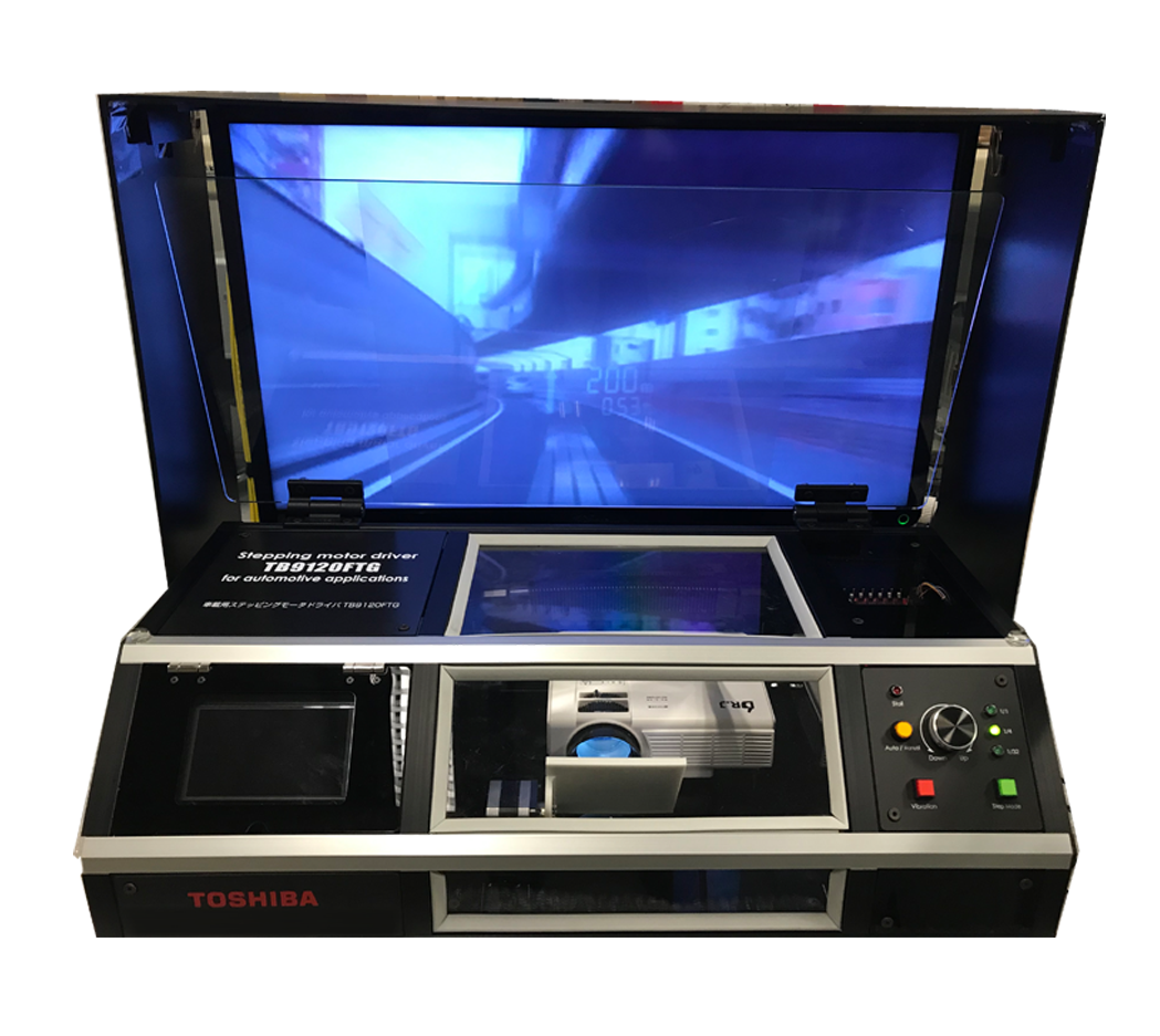
Stepping motor driving IC
- A projector emits Head-up Display typical information content
- The light-beam is reflected to an upwards oriented screen
- A stepper motor controlled mirror moves the content up/downcontrol)
Key product:
Check for more:
| Features | Advantages | Benefits |
|---|---|---|
|
|
|
DC Motor Controller For Wing Mirrors With Integrated Current Monitor
Device offers highly efficient operation
Integrated DC motor drivers for automotive applications can be found in a variety of automotive application fields. Featuring a 1 channel H-Bridge with integrated MOSFETs, Toshiba’s TB9051FTG (MIKROE ClickboardTM TB9051FTG) is able to drive up to 28V and 5A to the attached motor. It can be used e.g. inside an automotive grade door mirror, controlling the motorized fold and open of the mirror. Besides the device is also suitable for applications such as electronic throttle and valve control. It is AEC-Q100 qualified and uses various built-in failure detection features for functional safety. These include over current, over heat, low voltage and high voltage detection circuits. TB9051FTG offers a compact P-QFN28 package (6mm × 6mm), well suited for small mounting boards.
Expand Your Knowledge
electronicnet.de: Interview
Armin Derpmanns, Vice President Marketing & Operations at Toshiba Electronics Europe, spoke with Iris Stroh from Markt&Technik, a renowned electronics publication in Germany. (*Interview in German language. Copyright: Markt & Technik, electronicnet.de)
We are Toshiba Europe
Discover the story of Toshiba Europe and see how the company unites the team by a shared commitment to innovation and excellence, working together to create a smarter, more secure, and sustainable future, inspiring positive change.
The Electropages Podcast
In this podcast with host Robin Mitchell Armin Derpmanns, Vice President of Marketing and Operations at Toshiba, highlights Toshiba’s focus on power semiconductors, the growing role of silicon carbide, and the strategic move towards sustainability and digitalization.
Semiconductor, Battery, HDDs & Superconducting Motors
Whitepapers, High Voltage Laboratory & More Articles
Whitepapers
Find detailed information about the benefits of our MOSFET-portfolio including SiC, HV- and LV-MOSFETs at our innovation centre.
High Voltage Laboratory
Toshiba's high voltage laboratory in EMEA allows us to address application-related questions from customers more rapidly.
Power Focus Interview
Learn more about TEE’s focus on power in our interview* with the magazine Markt & Technik. *Please note that the interview is in German..
Podcast Analog ICs
In the podcast Passion for technology the need for miniaturisation of analog devices is discussed.
Innovation Centre, e-Learning & more