- General Top
- SEMICONDUCTOR
- STORAGE
- COMPANY
-
My ToshibaSemicon
- Semiconductor Top
-
ApplicationsAutomotive
Body Electronics
xEV
In-Vehicle Infotainment
Advanced Driver-Assistance Systems (ADAS)
Chassis
IndustrialInfrastructure
BEMS/HEMS
Factory Automation
Commercial Equipment
Consumer/PersonalIoT Equipment
Healthcare
Wearable Device
Mobile
Computer Peripherals
-
ProductsAutomotive Devices
Discrete Semiconductor
Diodes
Transistors
Logic ICs
Analog Devices
- Automotive SmartMCD™ (Integreted SoC Conbining Microcontroller and Driver)
- Automotive Brushless Motor Driver ICs
- Automotive Brushed DC Motor Driver ICs
- Automotive Stepping Motor Driver ICs
- Automotive Driver ICs
- Automotive System Power Supplies ICs
- Automotive audio power amplifier ICs
- Automotive Network Communication
Digital Devices
Wireless Devices
※
 : Products list (parametric search)Power Semiconductors
SiC Power Devices
※
: Products list (parametric search)Isolators/Solid State RelaysPhotocouplers
Digital Isolators
Solid State Relays
Fiber Optic Transmitting Modules
※
: Products list (parametric search)MOSFETsIGBTs/IEGTsBipolar Transistors※
: Products list (parametric search)Diodes※
: Products list (parametric search)MicrocontrollersMotor Driver ICsIntelligent Power ICs※
: Products list (parametric search)Power Management ICsLinear ICs※
: Products list (parametric search)General Purpose Logic ICsLinear Image SensorsOther Product ICsOther Product ICs
※
: Products list (parametric search) -
Design & Development
Design & Development
Innovation Centre
At the Toshiba Innovation Centre we constantly strive to inspire you with our technologies and solutions. Discover how to place us at the heart of your innovations.
-
Knowledge
Knowledge
Highlighted Topics
Further Materials
Other
- Where To Buy


- Part Number & Keyword Search
- Cross Reference Search
- Parametric Search
- Stock Check & Purchase
This webpage doesn't work with Internet Explorer. Please use the latest version of Google Chrome, Microsoft Edge, Mozilla Firefox or Safari.
require 3 characters or more. Search for multiple part numbers fromhere.
The information presented in this cross reference is based on TOSHIBA's selection criteria and should be treated as a suggestion only. Please carefully review the latest versions of all relevant information on the TOSHIBA products, including without limitation data sheets and validate all operating parameters of the TOSHIBA products to ensure that the suggested TOSHIBA products are truly compatible with your design and application.Please note that this cross reference is based on TOSHIBA's estimate of compatibility with other manufacturers' products, based on other manufacturers' published data, at the time the data was collected.TOSHIBA is not responsible for any incorrect or incomplete information. Information is subject to change at any time without notice.
require 3 characters or more.
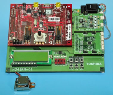
Control using MCU
The operation of an ultrasonic motor highly depends on its material, shape, size, and so on. Especially the supply voltage values and phases should be adjusted to the characteristics of the individual motor. The motor controller requires high resolution (finely adjustable) one-shot pulse.
Toshiba offers one of the best solutions to control fine adjustment of supply voltages by embedding a high resolution PPG (Programmable Pulse Generator) output to a microcontroller (TX03 Series M340 Group)
High Resolution PPG (Programmable Phase Generator) Output
A High resolution PPG output is an output of one-shot pulse which is generated by a timer embedded in a microcontroller. The frequency and the duty are modified by as fine as 6.25ns resolution. The leading edge and trailing edge of the pulse can be selected either rise-and- fall or fall-and-rise, respectively.
The first transition of one-shot pulse is a leading edge,
and the second, a trailing edge.
Each edge can be either a rising edge or a trailing edge.
At first operation of the timer is explained.
The timer in the PPG circuit includes several registers; a period register CP0, a leading timing register CP1, and a trailing register CP2. A free-running counter is also in the timer. This counter becomes “0” when reset, and increments by every clock. The count value is compared to CP0, CP1, and CP2 every clock timing.
The counter starts at ‘0’ and continue to increment. When the value of the counter becomes the same value of CP1, it generates a leading edge of the output pulse. The leading edge can be selected from a rising edge or a falling edge. Supposing it is a rising edge now, the output changes from low level to high at CP1 value timing.
The counter keeps incrementing and becomes the same value of CP2 next. This is the time of the trailing edge occurrence. This time the edge must be a falling edge because the leading edge was a rising one. The output transits from high level to low.
The counter increments more and becomes CP0 value, which resets the counter to ‘0’. And the counter increments again.
This process makes one shot pulse with CP0 period, the rising edge at CP1 and the falling edge at CP2. The increment clock has the period of 6.25ns minimum which is the least resolution time of the pulse width.
If the leading edge is set to a falling edge, the trailing edge becomes a rising edge automatically, and the output is high level initially, falls at the leading edge time, and rises at the trailing edge time.

Now, interlock PPG mode is explained.
The interlock mode is a smart solution
for fine adjustment of the pulses.
Interlock PPG mode
Two independent timers with high resolution PPG output are implemented in Toshiba microcontroller. Two different one-shot pulses are generated and output to different terminals.
Those two timers can also work together in interlock operation.
In this mode, though each output can have different duties independently, the period must be identical. The phase difference can be selected from -180 degrees to +180 degrees with as fine as 6.25ns resolution at minimum.
The operation of the interlock mode is as follows.
There are two timers in this mode, one is referred to as Timer 0, and the other, Timer 1, to distinguish from each other. The period register of Timer 0 CP00, the leading edge register CP01, and the trailing edge register CP02 operate in the same way as the explanation above. The leading edge and trailing edge of the pulse can also be either rise-and- fall or fall-and-rise in the same way, respectively.
On the other hand, the period register of Timer 1, CP10, is ignored. The period of Timer 1 is determined by the period register of Timer 0, CP00 in order for both Timer 0 and 1 to operate in the same period. The increment clock of each timer is identical, otherwise, they cannot operate in interlock mode.
The leading edge and trailing edge of Timer 0 and Timer 1 are set independently not only those values but also rising or falling edges.
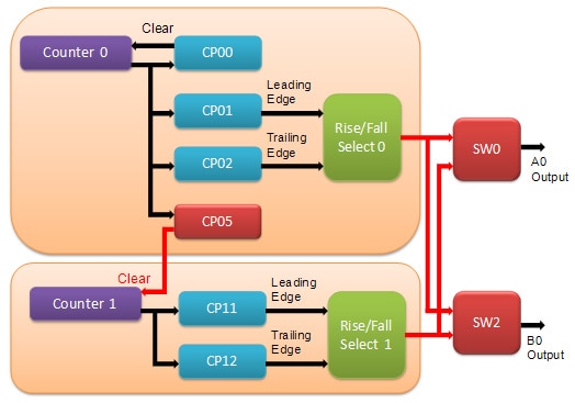
A new register C05 is introduced in the interlock mode. The function of the register is to keep a value to reset the counter of Timer 1 when the counter of Timer 0 becomes C05 value.
Let’s check what kind of pulses would come out from the terminals in the interlock mode, when the values in the registers have the following condition;
CP01 = CP11 < CP02 = CP12 < CP00、CP05 < CP01
And another condition is that the leading edge and the trailing edge of both Timer 0 and Timer 1 are a rising and falling, respectively. In this case the waveforms of output A0 and output B0 have the same period and the same duty with the phase difference by CP05 value.
(1) The initial point should be the counter of Timer 0 is CP00 value. It makes the counter reset. The counter of Timer 1 has some value now (the value will be known later).
(2) The two counters increment together synchronously. The counter of Timer 0 becomes CP05, then the counter of Timer 1 is reset.
(3) The counters continue to increment, and the counter of Timer 0 becomes CP01. The output A0 rises from low level to high level. The output B0 is still low level.
(4) Next, when the counter of Timer 1 becomes CP11, the output B0 rises. The output A0 remains high level.
(5) And, the counter of Timer 0 becomes CP02, and the output A0 falls.
(6) Next, when the counter of Timer 1 becomes CP12, the output B0 falls.
(7) Then, the increment continues and when the counter of Timer 0 becomes C00, the counter is reset, which returns to (1). At this time the counter of Timer 1 is the value of (C00-C05).
It returned to (1) now. Then it repeats to (7)
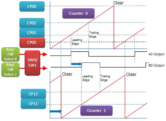
CP05 is important in this interlock PPG mode. As explained above Timer 1 is always behind by the value of CP05 from Timer 0. If the value of CP05 changes, the phase between the output 0 and the output 1 is shifted by the change value. This phase difference has as small as minimum 6.25ns resolution.
On the other hand, if the output 1 will be ahead of the output 0, the one-shot pulse generated by Timer 0 is transferred to the output 1 and that generated by Timer 1 to the output 0. That is, Timer operation remains the same and the exchange of the output 0 and 1 is done. This results in that the output 1 is ahead of output 0 by CP05.

When the phase difference is described with angle expression,
(C05÷C00)×360°
is the calculation formula.
C05 can take half of C00 at maximum.
The phase difference can be selected one in a wide range from -180°to +180°, but actually -90°to +90°is the value practically selected.
It was a long story. But I hope you understand well
the interlock PPG mode and its mechanism.
The circuit structure is rather simple, isn’t it?
Next, see a demonstration video of a super sonic motor
controlled by MCU.