


What is a diode
A diode is a semiconductor device that has two terminals, an anode and a cathode, and allows current to flow only in one direction (from the anode to the cathode, known as the forward direction). Current does not flow in the reverse direction, except for special cases, such as when a voltage exceeding the breakdown voltage is applied. It is an active component that has one p-n junction, or alternatively, one metal-semiconductor junction. Demand for general-purpose pn junction diodes has been declining recently due to their poor energy efficiency (they require VFxIF power when on) and slow switching speed, but they remain mainstream semiconductor devices.
Diode types and characteristics
Fig.1 is a conceptual diagram showing the classification relationships in a tree structure, with diodes at the top.
The diagram provides an overview of the overall relationship between diodes and their categories, focusing on differences in junction method. Each category shown in the diagram is further subdivided according to application and characteristics.
Diodes are broadly divided into PN junction diodes and metal-semiconductor junction diodes (Schottky barrier diodes) based on their type of junction. pn junction diodes are further divided into rectifier diodes and Zener diodes.
The following FAQ explains the types of diodes.
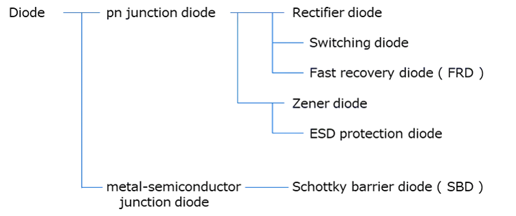
- pn junction diode
pn junction diodes are the most common type of diode, and come in a wide range of products, from general-purpose types to high-voltage and high-frequency types. A slightly more unusual type is the fast recovery diode (FRD), which has improved reverse recovery time.
As mentioned above, diodes only allow current to flow in one direction (forward direction), but if a large voltage is applied in the reverse direction, a continuous current will suddenly flow at a certain voltage.
This phenomenon is called Zener breakdown or avalanche breakdown. This behavior in ordinary diodes leads to deterioration and destruction, but Zener diodes are specially designed to utilize this phenomenon.
Zener diodes are known as constant-voltage diodes, but in recent years they have often been used for protection against electrostatic discharge (ESD). In particular, Zener diodes that specialize in ESD protection performance are called ESD protection diodes. We offer products that are suitable for various situations, such as high frequency and power sources.
Please also refer to the following FAQ and e-learning - Metal-semiconductor junction diode
Schottky barrier diodes (SBDs) are characterized by their low forward voltage and lack of reverse recovery time. However, because they involve the junction of dissimilar materials, metal and semiconductor (such as silicon), the leakage is slightly larger than that of pn junction diodes.
Please also refer to the following FAQs and e-learning materials.
- FAQ: What is a Schottky barrier diode (SBD)?
- e-learning: Basics of Schottky Barrier Diodes
- FAQ: What is a Schottky barrier diode (SBD)?
Diode structure and operation
Fig.2 shows a simplified structure diagram and symbols for a pn junction diode and a Schottky barrier diode.
In a pn junction diode, the junction surface is the boundary between the p layer and the n layer, and in a Schottky barrier diode, it is the boundary between the n-type semiconductor and the metal. An example of the external shape of a 2-pin surface-mount type is also shown, allowing you to see the corresponding relationship between the anode and cathode sides.
In terms of symbols, Schottky barrier diodes were sometimes shown with special symbols, but now they are unified with the symbols shown in the figure.
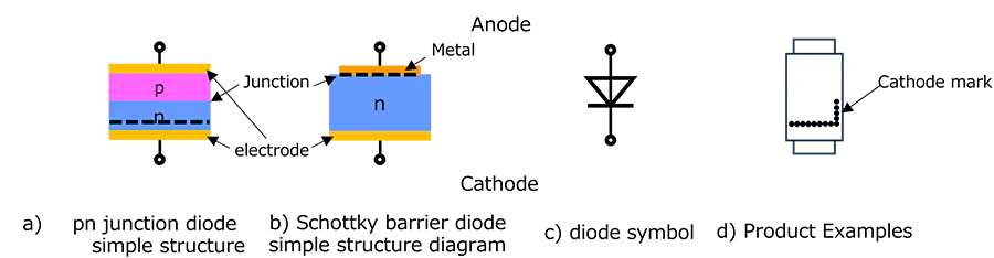
The structure of a pn junction diode is shown as a junction of a p-layer and an n-layer, as illustrated in Figure-2(a). In practice, however, the p-layer is formed by ion implantation or thermal diffusion of impurities (such as boron, B) into an n-type substrate. In some cases, an n-type layer may instead be formed by introducing impurities such as phosphorus (P) into a p-type substrate.
Schottky barrier diodes are generally constructed by evaporating metal particles onto an n-type. Although it is possible to configure an SBD with p-type, the leakage current is large and it is difficult to use it for general purpose, so n-type is mostly used.
As mentioned at the beginning, a diode only passes current in one direction. The direction in which current flows is called the forward direction, and the direction in which no current flows is called the reverse direction. Accordingly, voltage is defined as forward bias and reverse bias directions, as shown in the diagram.
Fig.3 shows a typical example of the current-voltage characteristics (IF-VF characteristics) of a diode, and a simple circuit configuration for measurement.
The measurement covers the low current region up to near the breakdown voltage (VR) in the reverse bias direction, and near the rise time in the forward bias direction.
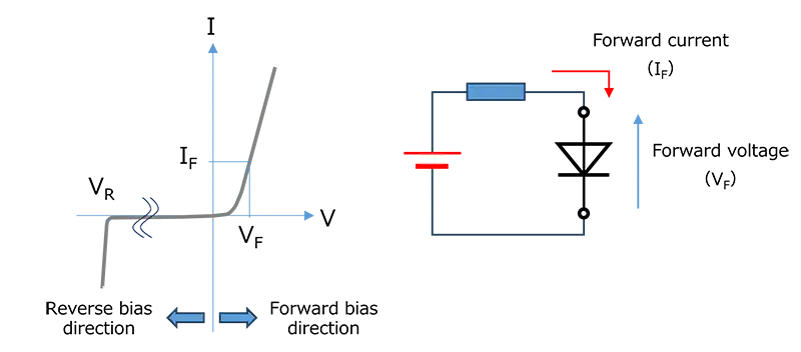
When a voltage is applied in the forward bias direction (anode side +) and the voltage is increased, current begins to flow at a certain voltage. This voltage varies slightly depending on the product, but is around 700mV for pn junction diodes and 200mV for Schottky barrier diodes. This voltage is called the forward voltage (VF). The current that flows currently is called the forward current (IF).
When a voltage is applied in the reverse bias direction (cathode side +) and the voltage is increased, current suddenly begins to flow at a certain voltage (breakdown voltage VR). This voltage also differs depending on the product, but for pn junction diodes it is tens to hundreds of volts, and for Schottky barrier diodes it is several tens of volts. This phenomenon in which current flows suddenly is called breakdown. Since a sudden increase in current occurs with a large voltage, breakdown in a typical diode can cause degradation or destruction of the element. Therefore, except for Zener diodes and ESD protection diodes that are intended to actively utilize this phenomenon, they cannot be used at voltages greater than the absolute maximum rated reverse voltage (VR).
The operation of diodes is also explained in the FAQ: "How do diodes work?". In addition, an explanation of their physical properties is given in the e-learning: "Basics of Schottky Barrier Diodes"
Diode applications
Diodes are the simplest semiconductor elements and have been used in a wide range of circuits. Some applications have been replaced by ICs, but here are some examples of where diodes are still used today.
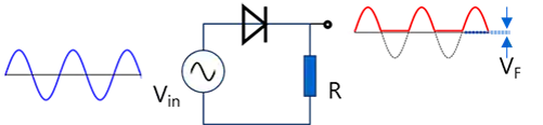
- Rectification:
Fig.4 shows a basic rectifier circuit consisting of a diode and resistor, and an example of the input and output waveforms for an AC input. When an AC signal is input, the output waveform has only one-directional components. This is called rectification.
This circuit is the most basic circuit, utilizing the one-way conduction characteristics of diodes. When an AC signal centered on GND is input, the diode turns on at a voltage level that is forward voltage (VF) higher than GND.
Even today, full-wave rectification circuits (diode bridges) that apply this technique are used in many electronic devices.
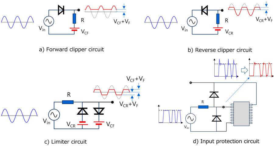
Clipper circuits, limiter circuits:
Fig.5 shows examples of a forward clipper circuit, a reverse clipper circuit, and a limiter circuit that combines them, as well as an example configuration of an input protection circuit used in ICs, etc.
The basic idea of using a diode to limit the amplitude of the signal voltage is shown together with the input and output waveforms.
There are forward clippers and reverse clippers in clipper circuits. One application of this is the limiter circuit. This is still used today for input protection (overvoltage protection) of ICs.
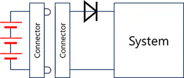
- Reverse battery protection / Reverse current protection:
Fig.6 shows a typical circuit configuration example for protecting a circuit from reverse battery connection.
This shows the basic idea behind inserting a diode in series with the power supply line to prevent reverse voltage from being applied to the main unit even if the polarity is accidentally connected in reverse.
In cases where there is a possibility of accidentally connecting the polarity in reverse, such as with batteries, a diode is connected in series to the power line. Since normal pn junction diodes have a large insertion loss, Schottky barrier diodes with a small VF are used. However, care must be taken regarding leakage current during reverse bias.
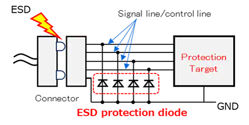
- ESD protection:
Fig. 7 shows a typical circuit configuration example for protecting a circuit from electrostatic discharge (ESD) that intrudes from the outside. It shows the basic idea of using protective elements to protect a circuit from ESD that intrudes through an external interface.
ESD protection diodes are used by connecting between the signal line and GND of an externally exposed terminal (such as a USB terminal) into which ESD may penetrate. An ESD protection diode or Zener diode specially designed for this purpose is used.
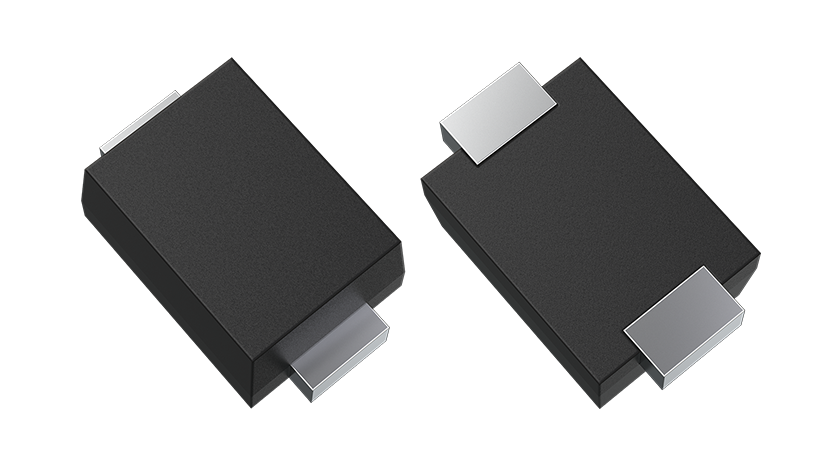
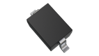
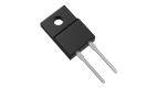
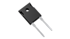
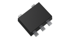
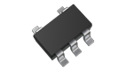
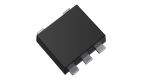
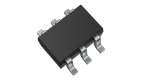
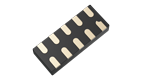
Diode packages
Diode packages are mainly two-pin packages with two terminals, an anode and a cathode. We offer mainly surface mount packages ranging from ultra-small to large. There are also multi-pin packages with multiple built-in diodes.
Some examples are shown below.
For details on package dimensions, etc., please refer to the following page.
Diode Package
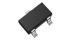
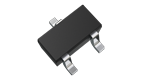
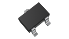
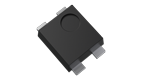
2pins
Mounting:Surface Mount


Mounting:Through Hole

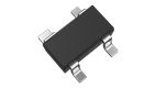
3pins
Mounting:Surface Mount


Mounting:Through Hole

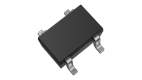
4pins
Mounting:Surface Mount
5pins
Mounting:Surface Mount
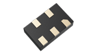

6pins
Mounting:Surface Mount
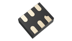


10pins
Related Links
For products, please refer to the following links.


* Company names, product names, and service names used in this FAQ may be of their respective companies.