- General Top
- SEMICONDUCTOR
- STORAGE
- COMPANY
-
My ToshibaSemicon
- Semiconductor Top
-
ApplicationsAutomotive
Body Electronics
xEV
In-Vehicle Infotainment
Advanced Driver-Assistance Systems (ADAS)
Chassis
IndustrialInfrastructure
BEMS/HEMS
Factory Automation
Commercial Equipment
Consumer/PersonalIoT Equipment
Healthcare
Wearable Device
Mobile
Computer Peripherals
-
ProductsAutomotive Devices
Discrete Semiconductor
Diodes
Transistors
Logic ICs
Analog Devices
- Automotive SmartMCD™ (Integreted SoC Conbining Microcontroller and Driver)
- Automotive Brushless Motor Driver ICs
- Automotive Brushed DC Motor Driver ICs
- Automotive Stepping Motor Driver ICs
- Automotive Driver ICs
- Automotive System Power Supplies ICs
- Automotive audio power amplifier ICs
- Automotive Network Communication
Digital Devices
Wireless Devices
※
 : Products list (parametric search)Power Semiconductors
SiC Power Devices
※
: Products list (parametric search)Isolators/Solid State RelaysPhotocouplers
Digital Isolators
Solid State Relays
Fiber Optic Transmitting Modules
※
: Products list (parametric search)MOSFETsIGBTs/IEGTsBipolar Transistors※
: Products list (parametric search)Diodes※
: Products list (parametric search)MicrocontrollersMotor Driver ICsIntelligent Power ICs※
: Products list (parametric search)Power Management ICsLinear ICs※
: Products list (parametric search)General Purpose Logic ICsLinear Image SensorsOther Product ICsOther Product ICs
※
: Products list (parametric search) -
Design & Development
Design & Development
Innovation Centre
At the Toshiba Innovation Centre we constantly strive to inspire you with our technologies and solutions. Discover how to place us at the heart of your innovations.
-
Knowledge
Knowledge
Highlighted Topics
Further Materials
Other
- Where To Buy


- Part Number & Keyword Search
- Cross Reference Search
- Parametric Search
- Stock Check & Purchase
This webpage doesn't work with Internet Explorer. Please use the latest version of Google Chrome, Microsoft Edge, Mozilla Firefox or Safari.
require 3 characters or more. Search for multiple part numbers fromhere.
The information presented in this cross reference is based on TOSHIBA's selection criteria and should be treated as a suggestion only. Please carefully review the latest versions of all relevant information on the TOSHIBA products, including without limitation data sheets and validate all operating parameters of the TOSHIBA products to ensure that the suggested TOSHIBA products are truly compatible with your design and application.Please note that this cross reference is based on TOSHIBA's estimate of compatibility with other manufacturers' products, based on other manufacturers' published data, at the time the data was collected.TOSHIBA is not responsible for any incorrect or incomplete information. Information is subject to change at any time without notice.
require 3 characters or more.
Are the collector and emitter terminals of a bipolar transistor interchangeable?
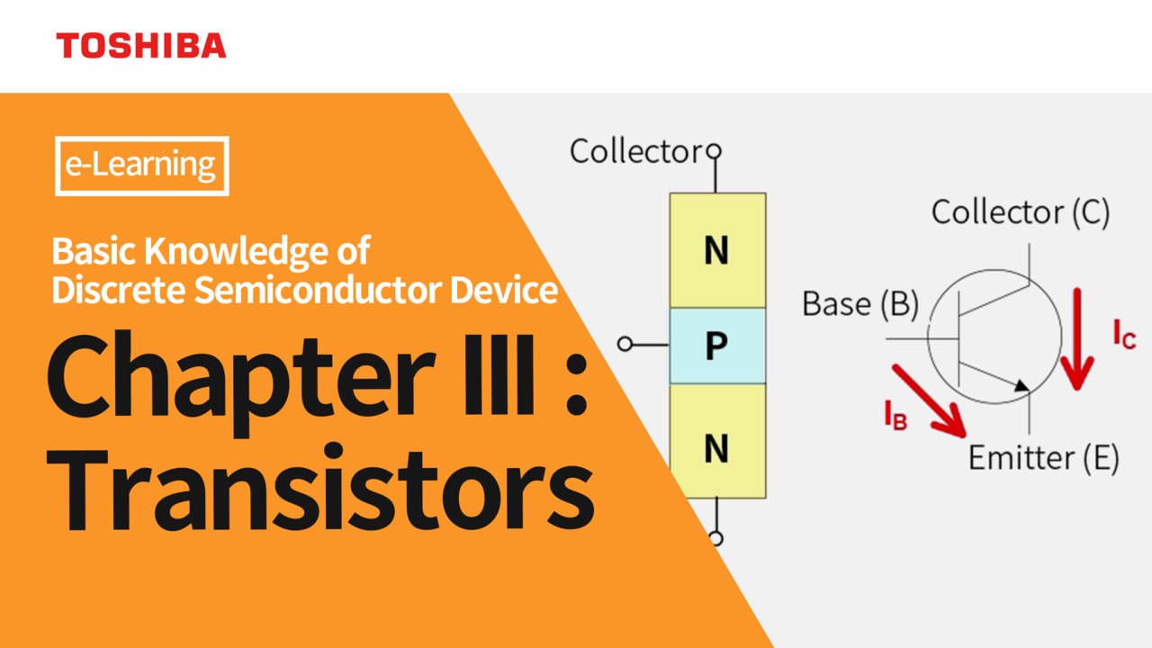
Bipolar junction transistors (BJTs) are designed to provide the optimum performance when they are correctly connected. In reverse connection, it behaves as a poor performance (low hFE) transistor. However, the voltage that can be applied to the collector-base voltage is very low. This voltage cannot exceed the absolute maximum rating (VEBO) (Table. 1). Interchanging the collector and emitter terminals not only degrades the transistor performance but also might cause permanent damage to the device.
Generally, bipolar transistors are designed in such a manner as to achieve high hFE. To accomplish this, numerous majority carriers (electrons in the case of npn transistors) in the emitter must diffuse into the base region and then be efficiently swept across the base region into the collector. It is also necessary to control the depletion layer in the collector region in order to increase a transistor’s withstand voltage (i.e., collector-base voltage, VCBO). These conditions are fulfilled by:
- making the dopant concentration in the emitter region higher than that in the base region.
- reducing the thickness of the base region.
- reducing the dopant concentration in the collector region.
Therefore, the dopant concentrations in the three semiconductor regions have the following relationship: emitter >> base > collector.
A normal transistor maintains a high breakdown voltage (VCBO / VCEO) due to a low-concentration collector. If connected in reverse, the high-concentration emitter will act as the collector, and the voltage that can be applied (VEBO) will be extremely low.
If the connections of the collector and emitter terminals are reversed, the above relationship is not satisfied. In this case, hFE decreases, making it impossible for a bipolar transistor to function as intended and possibly causing the base current to exceed its specified rating. Moreover, because of the decreased VCEO, the transistor might break down when it turns off. As a result of the foregoing, a reverse-connected transistor might be permanently damaged.
Typical bipolar transistors must be connected in the normal direction, except for muting transistors* that are designed for reverse connection.
* At present, Toshiba does not provide muting transistors.

Related Links
The following documents also contain related information: