


What is a transistor
A transistor is a semiconductor device that has at least three terminals and functions to amplify electrical signals and act as a switch. Depending on their structure, they are broadly divided into bipolar transistors (BJT) and field effect transistors (FET). In addition, there are also insulated gate bipolar transistors (IGBT), which have MOSFET input stages and BJT characteristics in the output stages.
Types and characteristics of transistors
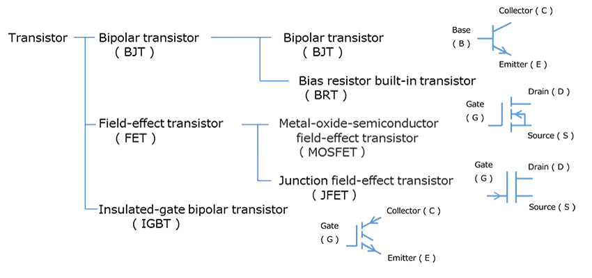
Figure-1 shows the classification of transistors.
In the figure, they are organized into a tree structure starting from the transistor, and are classified into bipolar transistors (BJT), field-effect transistors (FET), and insulated-gate bipolar transistors (IGBT).
There is also an explanation in the FAQ below.
FAQ: What types of transistors are available?
- Bipolar Junction Transistor (BJT)
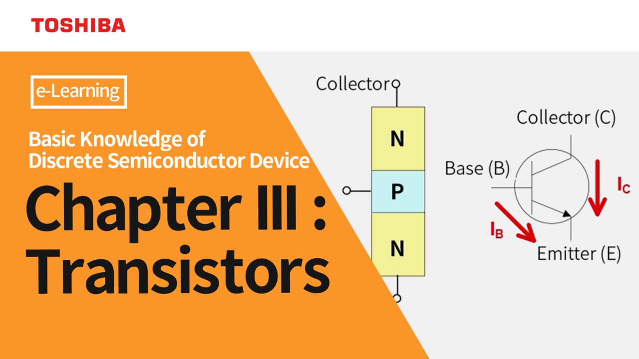
BJT has two pn junctions. It uses both electrons and holes as charge carriers. For this reason, it is called a bipolar transistor. BJT has three terminals: base, collector, and emitter. There are two types: NPN-BJT and PNP-BJT.
The collector current flows in proportion to the current (base current) that flows from the base to the emitter. For this reason, BJT is called a current-controlled element. The transistor is off when the base current does not flow.
Normally, a voltage is used as the control signal for the BJT, and the control voltage is converted to a current by a resistor and input to the base (Fig. 3). Bias Resistor built-in Transistor (BRT), which has this resistor built in and is mainly used as a switch, is a type of bipolar transistor.
Unlike MOSFET, BJT needs to pass current to the base, so the power consumed by the device is larger than that of MOSFET. Although the switching speed is slow, it is easy to make it high voltage resistant. In addition, it is characterized by its easy gain and high amplification factor. BJTs are used in circuits that require a high amplification factor. Due to the conductivity modulation effect (minority carrier accumulation effect), BJTs have a low voltage drop at saturation, but this effect also has the disadvantage of lengthening the transition time from on to off.
Please also refer to the following FAQs: - Field Effect Transistor (FET)
FETs are transistors that do not have a pn junction in the path through which current flows. Only electrons or holes are used as charge carriers. For this reason, they are also called unipolar transistors in contrast to bipolar transistors. There are two types of FETs: metal-oxide-semiconductor field-effect transistors (MOSFETs), which are mainly used for switching, and junction field-effect transistors (JFETs), which are mainly used in amplifiers.
FETs have three terminals: gate, drain, and source.
The voltage applied between the gate and source (gate voltage) turns the element on and off. In the saturation region, the magnitude of the output current changes depending on the magnitude of the gate voltage. For this reason, FETs are called voltage-controlled elements.
The gate terminal is insulated from the other terminals, so no current flows except for the current that charges the parasitic capacitance. Its features include low drive current and high-speed switching.
Please also refer to the following FAQs:- FAQ: What is a MOSFET?
- FAQ: What is a JFET?
- Insulated Gate Bipolar Transistor (IGBT)
IGBT is a device that has the characteristics of MOSFET and BJT. It is a product that combines two characteristics of MOSFETs: high-speed switching and BJTs: low on-state voltage (low saturation voltage). IGBTs use electrons and holes as charge carriers in operation, so they are sometimes classified as bipolar transistors.
IGBTs have three terminals: gate, collector, and emitter.
Please also refer to the following FAQs- FAQ: What is an IGBT?
Structure of transistor
A simplified structural diagram and symbols for various transistors are shown in Fig. 2.
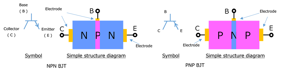
- Bipolar Junction Transistor (BJT)
An NPN BJT has a p-layer base sandwiched between the n-layer collector and emitter. A PNP BJT has an n-layer base sandwiched between the p-layer collector and emitter.
To increase the DC current gain hFE, the base is very narrow (thin) and the impurity concentration is collector < base << emitter.
The symbol and simplified structural diagram of a bipolar transistor (BJT) are shown in Figure-2 (a). In the simplified structural diagram, for example, an NPN type is shown with a thin P-layer base sandwiched between N-layer emitter and collector, but this is a schematic diagram to make it easier to understand the operating principle, and does not directly represent the physical structure of an actual BJT.
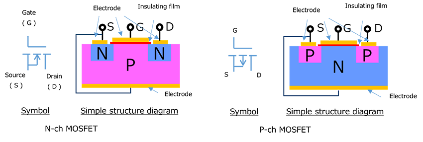
- Metal Oxide Semiconductor Field Effect Transistor (MOSFET)
In an N-ch MOSFET, the drain and source, which are n layers, are embedded in the p layer. (There is also a vertical structure, but here we will explain the basic horizontal structure.) For the gate, which serves as the control terminal, an insulating film (oxide film) is formed directly above the p-layer, covering one end of the drain and source n-layers, and the gate electrode is placed on top of it. When voltage is applied to the gate, a current path is formed in the p-layer in contact with the insulating film, electrically connecting the n-layer drain and source. Because a path (channel) equivalent to that of the n-layer is formed in the p-layer in this way, it is called an n-channel (N-ch) MOSFET. A P-ch MOSFET has a structure in which the drain and source (p layers) are embedded in the n layer. The gate electrode is placed directly above the n-layer through an insulating film, covering one end of the p-layer for the drain and source.
The symbol for a MOSFET and a simplified structural diagram are shown in Figure-2 (b). The figure shows an N-channel MOSFET and a P-channel MOSFET as cross-sectional views of a lateral structure, with the N-channel MOSFET using a P-type substrate and the P-channel MOSFET using an N-type substrate. The source (S) and drain (D) are formed in the substrate, and the gate (G) is placed on top of them via an insulating film, allowing the conduction state between the drain and source to be controlled by the gate voltage.
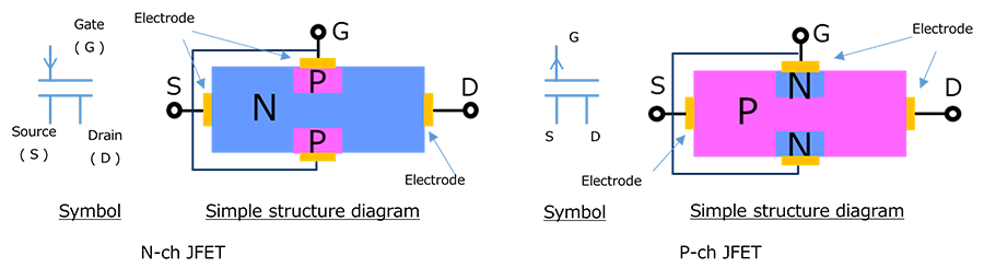
- Junction Field Effect Transistor (JFET)
N-ch JFET has a p-layer, which is the gate, embedded in the n-layer, which is the drain and source. The n-layer and p-layer that form the junction are used in reverse bias, so no current flows from the p-layer to the n-layer. Since the current path is the n-layer, it is called an n-channel (N-ch). This n-layer acts as a resistor.
When a voltage is applied to the gate, the depletion layer expands in proportion to the voltage, narrowing the current path between the gates and increasing the resistance value.
The symbol for a JFET and a simplified structural diagram are shown in Figure-2 (c). For example, an N-channel JFET is expressed as a structure in which an N-layer is used as the substrate and P-layers are placed above and below it. However, this structural diagram is a schematic diagram intended to make it easier to understand the operating principle of a JFET, and it differs in some respects from the actual device structure. A distinctive feature of a JFET is that the channel width is controlled by the gate (G).
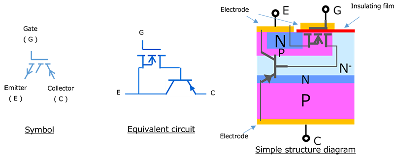
- Insulated-gate bipolar transistors (IGBT)
An IGBT is a composite device consisting of a MOSFET and a BJT. The input section has a MOSFET structure with fast switching and low drive current, while the output section has a BJT structure capable of high current and high withstand voltage. This allows for faster switching speeds than a BJT, and a device with higher withstand voltage and lower on-resistance than a MOSFET.
The symbol for an IGBT and a simplified structural diagram are shown in Figure-2 (d). The figure shows an equivalent circuit for an N-ch IGBT as an example, along with a simplified structural diagram that overlays that equivalent circuit. An IGBT is a device that uses an N-ch MOSFET as its basic structure and combines elements of a bipolar transistor in the output stage, and is characterized by combining the high-speed switching characteristics of a MOSFET with the low on-voltage characteristics of a bipolar transistor.
Operation of transistor
- Bipolar Junction Transistor (BJT)
For an NPN BJT, when a voltage is applied to the collector (C) and a voltage (on voltage) of about 0.7V is applied between the base (B) and emitter (E), the Base current flows and the BJT turns on. When VBE becomes lower than this on voltage, the BJT turns off. As this collector-emitter voltage VCE approaches zero, the DC current gain hFE of the BJT decreases.
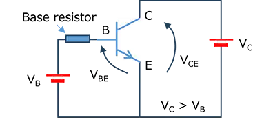
However, because the mutual conductance (gm: change in collector current with respect to change in voltage between the base and emitter) of the BJT is large, it is not practical to apply a voltage directly to the base and control it with voltage. In the circuit shown in Fig. 3, a base resistor is inserted and the voltage applied to the base terminal is converted into a current. It is controlled by the change in this current.
Figure-3 shows an example of the simplest bias circuit for an NPN-BJT. In the diagram, a base bias voltage VB is applied to the base, with a base resistor inserted in series. A bias voltage VC is also applied between the collector and emitter, with VC>VB. In this circuit, no emitter resistor is inserted, as the base resistor limits the base current.
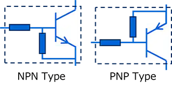
There is also a bias resistor built-in transistor (BRT, Figure-4) that has an external resistor built in and is intended for switching purposes.
Figure-4 shows the equivalent circuit of a BRT (Built-in Resistor Transistor). A BRT is a device that incorporates the base resistor required when using a BJT as a switch, and can be driven without an external resistor. This reduces the number of external components and the mounting area, contributing to a simpler circuit.
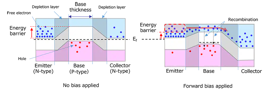
Let's think about the operation of BJT from a physical perspective. A transistor is a current-controlled element that amplifies the base current to pass the collector current, but here we will explain it in terms of the voltage applied to the base rather than the base current. Figure-5 shows the energy band diagram of an NPN transistor.
Figure-5 shows the state when there is no bias and when a forward bias is applied between the base and emitter. When there is no bias, the energy barrier formed at the pn junction between the emitter and base prevents free electrons in the emitter from moving to the base, and no current flows between the collector and emitter. On the other hand, when a forward bias is applied between the base and emitter, this energy barrier is lowered, and some of the free electrons in the emitter pass over the base and flow into the collector. This is the collector current.
If the impurity concentrations of the emitter, base, and collector of an NPN transistor are NE, NB, and NC, respectively, then NE >> NB > NC. There are free electrons or holes in proportion to this impurity concentration. In addition, the energy of each free electron follows the Fermi distribution (Fermi-Dirac distribution).
In a no-bias state, a built-in potential (the energy difference between the lowest limit of the emitter's conduction band and the lowest limit of the base's conduction band) occurs at each pn junction due to the generation of a depletion layer, creating an energy barrier. The emitter electrons cannot cross this barrier, and no current flows between the collector and emitter.
In the circuit shown in Figure 3, applying a forward bias (VBE higher than the on-voltage) between the base and emitter lowers the energy barrier.
Some of the free electrons (free electrons in the emitter with energy higher than this energy barrier) cross the barrier and diffuse into the base. At the same time, holes are injected into the base as base current. However, since NE >> NB, the number of free electrons diffused from the emitter is much greater than the number of holes in the base. Some of the diffused free electrons recombine with holes, but because the number of holes is small compared to the number of free electrons (difference in impurity concentration between the base and collector) and the thickness (width) of the base is thin, most of them drift due to the electric field between the base and collector and flow into the collector. This is the collector current.
- Metal Oxide Semiconductor Field Effect Transistor (MOSFET)
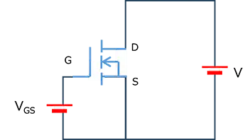
Figure-6 shows an example of the simplest bias circuit for an N-channel MOSFET. The diagram shows a configuration in which a bias voltage VGS is applied between the gate and source, and a bias voltage V between the drain and source. A channel is formed by the gate voltage VGS, but because the gate is insulated, no gate current flows. Therefore, a resistor to limit current, as with a BJT, is not required. However, a resistor may be inserted at the gate to adjust the rise time or prevent oscillation.When a voltage (VGS) above the threshold is applied between the gate and source, conduction occurs between the drain and source with a small resistance RDS(ON), and the MOSFET turns on. When VGS falls below the threshold, conduction does not occur between the drain and source, and the MOSFET turns off.
The gate terminal of a MOSFET is insulated, so when turning it off, the gate voltage may not drop easily, and it may take some time. In such cases, a resistor may be inserted between the gate and source.
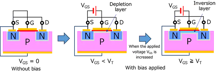
Figure-7 illustrates the bias conditions and inversion layer formation in an N-channel MOSFET when VGS is applied. The cross-sectional diagram shows three conditions: no bias (VGS = 0 V), a forward bias condition below the threshold voltage (VGS < VT), and a forward bias condition above the threshold voltage (VGS ≥ VT). For simplicity, the drain (D) and source (S) are shown externally shorted. For information on non-shorted conditions, see the FAQ below.
Without bias, there is no significant change in the P-type substrate directly below the gate. However, when VGS < VT, a depletion layer forms. Furthermore, when VGS ≥ VT, an inversion layer forms directly below the gate, forming a channel electrically connecting the drain and source.
N-type semiconductors usually have an excess of electrons, and P-type semiconductors usually have an excess of holes. When a voltage (VGS) is applied between the gate and source, the gate electrode and the P-type semiconductor directly below it act like a capacitor. When a voltage is applied between the gate and source, the electrode plate side becomes positively charged, and the P-type semiconductor side becomes negatively charged (electrons gather and there is an excess of electrons). In other words, negative charges gather on the surface of the P-type semiconductor directly below the gate, resulting in a state in which there are many free electrons. This state is called an inversion layer because it is a P-type semiconductor but has the same properties as an N-type semiconductor.
Fig. 7 shows the process by which an inversion layer is formed. A voltage VGS is applied to the gate from an unbiased state. First, before the inversion layer is formed, the holes in the P-type semiconductor that faces the gate electrode disappear, creating a depletion layer. When the voltage called the threshold voltage VT is reached, an inversion layer is formed. The source and drain are connected by this inversion layer. This inversion layer is called the channel, and in this example, since it is an N-type channel, it is an N-ch MOSFET.
When a MOSFET transitions from OFF to ON, a charging current is required for this capacitor, but once it is turned on, no current like the base current of a BJT is required, making it possible to save power. (However, MOSFETs for power applications have a large parasitic capacitor, and a drive circuit is required to quickly charge this capacitance and turn it on.)
- Junction Field Effect Transistor (JFET)
There are two operating modes: enhancement type (no current flows when the voltage between the gate and source is 0V) and depletion type (current flows when the voltage between the gate and source is 0V).
The operation of depletion type is explained below.
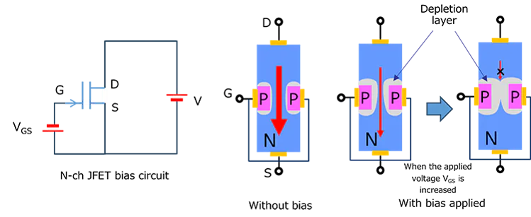
The N-ch JFET is an N-type semiconductor with a P-type semiconductor embedded as the gate. A pn junction is formed between the gate and the drain and source. This junction is used in a reverse bias state.
Fig.8 shows the change in the depletion layer as a function of the bias state in an N-channel JFET. The figure shows the simplest operating circuit, as well as cross-sectional views with no bias and with a bias applied. As the gate-source voltage VGS increases, the depletion layer formed at the gate junction expands, gradually narrowing the channel width.
When a reverse bias VGS is applied between the gate and source so that VG < VS, the depletion layer expands and the channel narrows. This inhibits the flow of current (it becomes resistant). If the reverse bias is further increased, the channel is blocked by the depletion layer.
- Insulated-gate bipolar transistors (IGBT)
IGBT is a device with a p-layer added to the drain (n-layer) of an N-ch MOSFET to serve as a collector. The input section is a MOSFET structure with fast switching and low drive current, and the output section is a BJT structure that allows for high current and high voltage resistance. This allows for a device that is faster than a BJT and has a higher voltage resistance and lower on-resistance than a MOSFET.
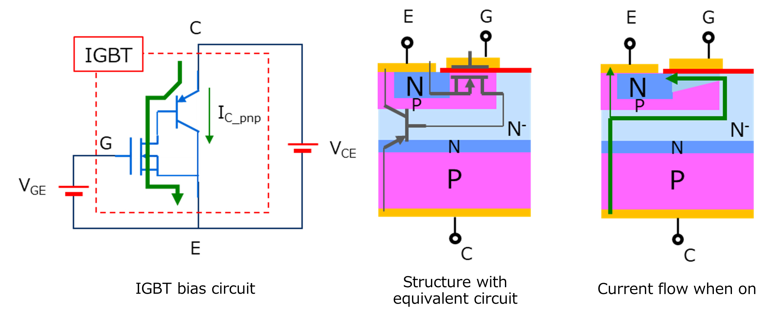
Figure-9 shows the current flow when an IGBT is on. (a) is a circuit diagram, (b) is a diagram of the IGBT equivalent circuit superimposed on a structural diagram, and (c) is a structural diagram showing the current path in the on state. When voltage is applied between the gate and emitter, the MOSFET in the input stage turns on, which activates the bipolar transistor in the output stage. The arrows indicate the current path when on.
For details on operation, please refer to the FAQ below.
FAQ: What is an IGBT?
As shown in the circuit diagram, apply voltage VGE between gate (G) and emitter (E), and voltage VCE between collector (C) and emitter (E). At this time, if VGE is equal to or higher than the threshold value of the N-ch MOSFET, the MOSFET turns on. This makes the base of the PNP transistor equipotential to the emitter, turning the PNP transistor on and causing a collector current IC to flow.
If VGE falls below the threshold value of the N-ch MOSFET, it turns off. However, a current called a tail current flows for a certain period of time before the IGBT turns off. This is due to the conductivity modulation effect that reduces the on-resistance when the device is turned on.
For more information on conductivity modulation, please refer to the following FAQ.
Applications of transistors
Transistors are used in all kinds of electronic devices and are mainly used in circuits that switch (on/off) or amplify electrical signals. Examples of switches include circuits that turn on/off at logic signal levels (up to 5V) and switching power supplies. Amplification circuits are also used not only for simple signal amplification but also for oscillation circuits. As you can see, transistors are used in a wide range of applications.
Both BJTs and MOSFETs can be used in these circuits. The choice between BJTs and MOSFETs depends on which characteristics (speed, loss, gain, etc.) are important in the circuit and what voltage, current, and frequency are used.
For reference, we have listed keywords related to each device.
-MOSFET: low power consumption, high-speed switching, high input impedance
-BJT: analog (linearity, high gain), low noise, turns on at low voltage (on voltage of about 0.7V)
Some circuit examples are shown below.
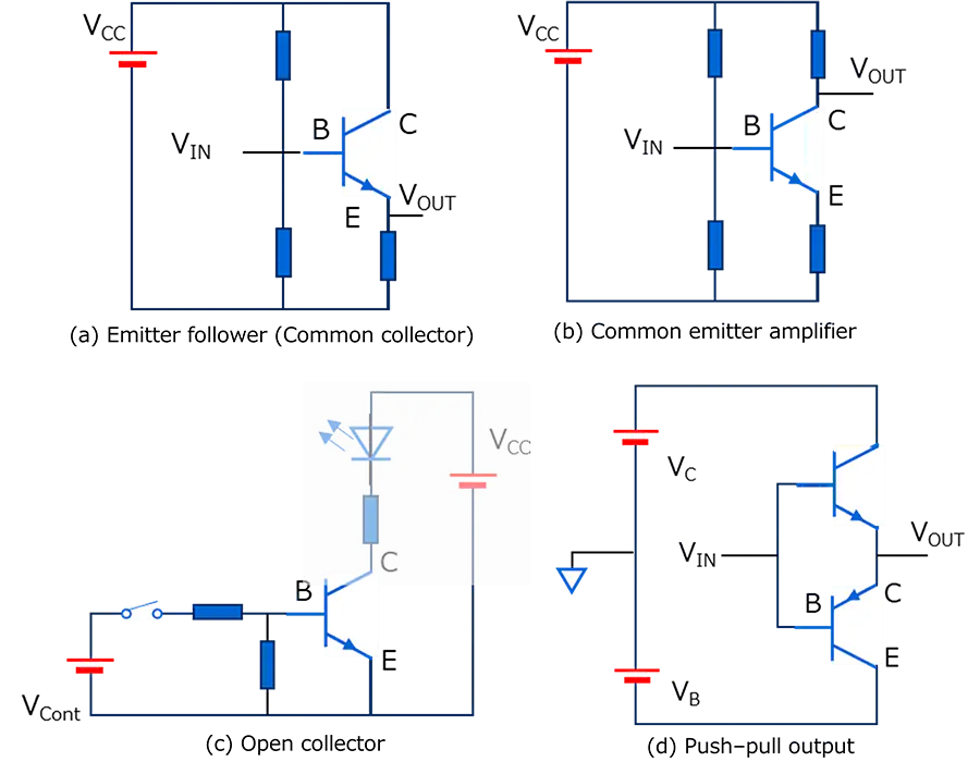
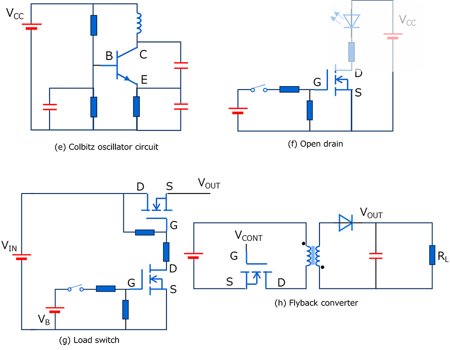
Fig. 10 Example of a circuit using a transistor
If you are interested in switching power supplies, please also refer to the following video.
[e-Learning] Full Bridge Converter - Basics of Switching Power Supplies (5)
[e-Learning] DC-DC Converter - Basics of Switching Power Supplies (6)
[e-Learning] Resonant Half Bridge Converter - Basics of Switching Power Supplies (7)
[e-Learning] Bridgeless PFC - Basics of Switching Power Supplies (8)
Transistor Package
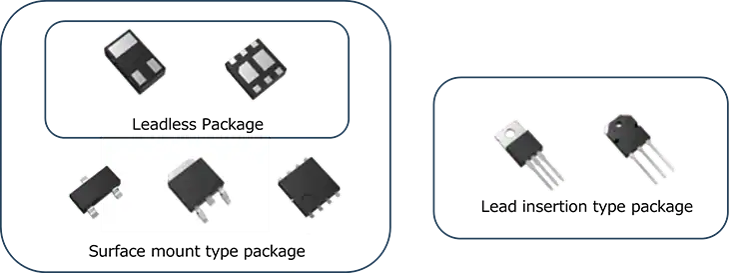
Toshiba's BJTs and MOSFETs are available in a wide range of packages, from small packages to packages for power applications. We also offer composite types such as 2-in-1.
Related Links
The following documents also contain related information.
Parametric Search
MOSFETs
Bipolar Transistors
FAQs

* Company names, product names, and service names used in this FAQ may be of their respective companies.