- General Top
- SEMICONDUCTOR
- STORAGE
- COMPANY
-
My ToshibaSemicon
- Semiconductor Top
-
ApplicationsAutomotive
Body Electronics
xEV
In-Vehicle Infotainment
Advanced Driver-Assistance Systems (ADAS)
Chassis
IndustrialInfrastructure
BEMS/HEMS
Factory Automation
Commercial Equipment
Consumer/PersonalIoT Equipment
Healthcare
Wearable Device
Mobile
Computer Peripherals
-
ProductsAutomotive Devices
Discrete Semiconductor
Diodes
Transistors
Logic ICs
Analog Devices
- Automotive SmartMCD™ (Integreted SoC Conbining Microcontroller and Driver)
- Automotive Brushless Motor Driver ICs
- Automotive Brushed DC Motor Driver ICs
- Automotive Stepping Motor Driver ICs
- Automotive Driver ICs
- Automotive System Power Supplies ICs
- Automotive audio power amplifier ICs
- Automotive Network Communication
Digital Devices
Wireless Devices
※
: Products list (parametric search)
Power SemiconductorsSiC Power Devices
※
: Products list (parametric search)
Isolators/Solid State RelaysPhotocouplers
Digital Isolators
Solid State Relays
Fiber Optic Transmitting Modules
※
: Products list (parametric search)
MOSFETsIGBTs/IEGTsBipolar Transistors※
: Products list (parametric search)
Diodes※
: Products list (parametric search)
MicrocontrollersMotor Driver ICsIntelligent Power ICs※
: Products list (parametric search)
Power Management ICsLinear ICs※
: Products list (parametric search)
General Purpose Logic ICsLinear Image SensorsOther Product ICsOther Product ICs
※
: Products list (parametric search)
-
Design & Development
Design & Development
Innovation Centre
At the Toshiba Innovation Centre we constantly strive to inspire you with our technologies and solutions. Discover how to place us at the heart of your innovations.
-
Knowledge
Knowledge
Highlighted Topics
Further Materials
Other
- Where To Buy
- Part Number & Keyword Search
- Cross Reference Search
- Parametric Search
- Stock Check & Purchase
This webpage doesn't work with Internet Explorer. Please use the latest version of Google Chrome, Microsoft Edge, Mozilla Firefox or Safari.
require 3 characters or more. Search for multiple part numbers fromhere.
The information presented in this cross reference is based on TOSHIBA's selection criteria and should be treated as a suggestion only. Please carefully review the latest versions of all relevant information on the TOSHIBA products, including without limitation data sheets and validate all operating parameters of the TOSHIBA products to ensure that the suggested TOSHIBA products are truly compatible with your design and application.Please note that this cross reference is based on TOSHIBA's estimate of compatibility with other manufacturers' products, based on other manufacturers' published data, at the time the data was collected.TOSHIBA is not responsible for any incorrect or incomplete information. Information is subject to change at any time without notice.
require 3 characters or more.
3D Thermal Fluid Analysis of MOSFETs: Expanding Simplified CFD Model Suitable for cooling simulation
One of the issues with power devices is heat generation, which causes various performance problems. Such thermal issues affect the reliability of power devices and peripheral circuits, therefore the thermal design by simulation using numerical fluid dynamics (CFD: Computational Fluid Dynamics) is important. Developing a device model for use with cooling simulation by CFD may take a lot of time depending on the device's structure.
Introduction
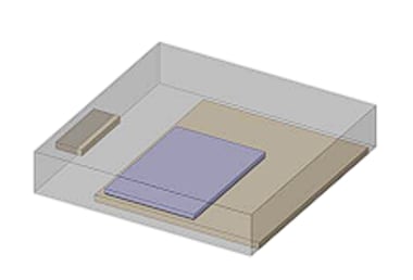
This article presents a simplified MOSFET model, shown in Figure 1, for use in cooling simulation, an example of how to check cooling simulation results, and the procedures (and links) to use them in cooling simulation.
Chapter 1: Why Thermal Analysis is Important for MOSFETs
The heat generated by MOSFETs may cause a variety of performance issues that impact the entire circuit, and in some cases, the functionality of peripheral devices. For example, thermal design guidelines exist for MOSFET placement in a chassis to minimize the effects of heat generated by MOSFETs.
Thermal analysis methods used in thermal design can be broadly classified into two categories:
- A simplified model, which converts the heat-flow path into an electric network, is used in SPICE simulations. This analysis considers only 1D behavior.
- A 3D model, generated from the device geometry, is used in cooling simulations by CFD. This method calculates the 3D behavior of the fluid, and the temperature distribution and fluid-flow can be visualized and checked, including inside that cannot be seen in the actual devices.
Reference link:
Chapter 2: CFD for Thermal Analysis
CFD combines numerical methods, data structures, and fluid dynamics to enable the analysis of fluid flow. CFD are widely used to confirm complex heat behaviors, such as thermal analyses and thermal managements of electronic components.
There are several benefits to using CFD for thermal analysis. For example, design modifications for board layouts and used components can be performed at a much lower cost through simulation compared to physical evaluation. Depending on the skill of CFD analyst, the analysis results can be highly accurate, enhancing the understanding of thermal behavior and interactions. CFD result also helps the analysis because it can visualize temperature and heat-flow, fluid-flow, etc.
Cooling simulation of MOSFET with CFD includes three different forms of heat transfer, as components are thermally complex on the circuit.
- Conduction by physical contact between components
- Thermal convection caused by moving fluids (e.g. air) around components
- Heat radiation, A component (e.g. MOSFETs) generates heat, and another object absorbs the heat
Simplified MOSFET model is helpful in analyzing such complex forms, and has benefits of shorter computation times and better convergence.
Toshiba prepares this simplified model as a "Simplified CFD Model."
Chapter 3: Simplified Model for MOSFET Cooling Simulation

The model shown in Figure 2 simplifies the actual component shapes that affect the heat-flow path into block shapes. The model consists of individual components (mold, chip, solder, gate-source pin, and exposed drain pad) and material properties of each component.
The abbreviations in Figure 2 have the following meanings.
- Mold: Mold
- Chip: Semiconductor chip
- SolderM: Solder for mounting semiconductor chip
- PinGS: Gate and source pin (common block)
- E-pad: Drain pad exposed at the bottom of the package
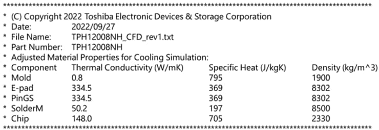
Simplified CFD Model requires the material properties of the components. Typical values for thermal conductivity, specific heat, and density are shown in Figure 3.
Chapter 4: Example of Cooling Simulation Using Simplified CFD Model
In this example, MOSFET's Simplified CFD Model is used to illustrate the results, including surface-temperature distribution, cross-sectional temperature distribution, thermal flow, and flow velocity.
4-1: Objective
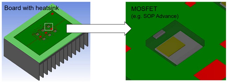
This example is a cooling simulation of a board model assuming an inverter circuit. The objective is to check the temperature of each MOSFET and its surroundings. Figure 4 shows six MOSFETs mounted on a board with heatsink. The material properties shown in Figure 3 are used for MOSFET.
4-2: Surface Temperature Distribution
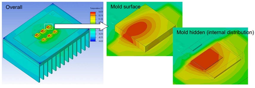
Figure 5 shows the surface temperature distribution of the entire board, the mold surface of the upper-right MOSFET, and the temperature distribution inside MOSFET.
From Figure 5, it can be seen that the heat generated by the MOSFET spreads to the outside of the board and heatsink. To understand the internal temperature distribution of the MOSFET, the display settings of the thermal fluid analysis tool allow for the visualization of temperatures within the device, such as the chip, which cannot be seen in the actual set.

The enlarged view in Figure 6 shows the internal temperature distribution of the board, including vias and Cu layers, without displaying the MOSFET itself. This example shows the temperature distribution around MOSFET located at the right edge on the board. The left image of the board temperature distribution shows the difference in temperature distribution with and without the influence of adjacent MOSFETs. Additionally, the board temperature decreases as the distance from the MOSFET increases. This indicates that the heat from each MOSFET’s Simplified CFD Model is transmitted to the board, affecting each other.
4-3: Cross-sectional Temperature Distribution
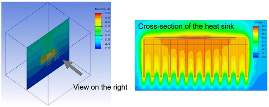
Figure 7 shows 2D cross-sectional temperature distribution of the heat sink taken from the center. It is comfirmed that the temperature is highest towards the center of the heatsink where the MOSFET is located. This indicates that the heat from Simplified CFD Model of each MOSFET that generated heat is being transferred to the heatsink.
Such a view helps to see how much heat energy and heat the heatsink can dissipate. It can see that heat is transmitted to the fin tips of the heat sink, centering on the area where the MOSFET is located.
4-4: Air (Fluid) velocity and flow
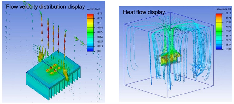
Figure 8 shows the velocity and flow of air (fluid) in the simulation chamber that was set during the analysis. The left side of the figure shows the velocity distribution, while the right side shows the flow paths.
Chapter 5: How to Use Simplified CFD Model
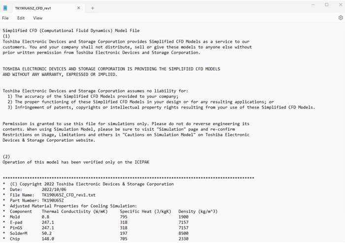
This Simplified CFD Model can be used with thermal fluid analysis tool. The models are available on our website, and you can check the available Toshiba MOSFETs via the reference links below. The downloaded file is provided in a compressed format and includes the following contents:
- A material properties text (.txt) file listing the thermal conductivity, specific heat, and density of the MOSFET. An example is shown in Figure 9.
- A STEP (*.stp) file containing the simplified 3D model of the MOSFET.
Importing these files to your thermal fluid analysis tool enables cooling simulation.
The steps to use the simplified CFD model in thermal simulations are as follows:
- Downloading compressed files of the purpose MOSFET and decompressing them to any folder
- Converting Simplified CFD Model to a simulation model with thermal fluid analysis tool's dedicated CAD Tool
- Importing simulation models to thermal fluid analysis tool
- Assign the property values described in the material property value text file to each part of the imported model.
- Running cooling simulation
For any questions regarding model import or material property settings, please contact your tool vendor.
Reference link:
Conclusion
Including MOSFETs in thermal simulations for thermal analysis is important, but the variety of MOSFET models can often make this process complex. This article introduced simplified MOSFET models that can be used in thermal simulations with CFD. All that is needed are the 3D models of the MOSFETs in STEP file format and the material properties of the MOSFETs, both of which can be downloaded for hundreds of types of MOSFETs from our website.


