
- General Top
- SEMICONDUCTOR
- STORAGE
- COMPANY
-
My ToshibaSemicon
- Semiconductor Top
-
ApplicationsAutomotive
Body Electronics
xEV
In-Vehicle Infotainment
Advanced Driver-Assistance Systems (ADAS)
Chassis
IndustrialInfrastructure
BEMS/HEMS
Factory Automation
Commercial Equipment
Consumer/PersonalIoT Equipment
Healthcare
Wearable Device
Mobile
Computer Peripherals
-
ProductsAutomotive Devices
Discrete Semiconductor
Diodes
Transistors
Logic ICs
Analog Devices
- Automotive SmartMCD™ (Integreted SoC Conbining Microcontroller and Driver)
- Automotive Brushless Motor Driver ICs
- Automotive Brushed DC Motor Driver ICs
- Automotive Stepping Motor Driver ICs
- Automotive Driver ICs
- Automotive System Power Supplies ICs
- Automotive audio power amplifier ICs
- Automotive Network Communication
Digital Devices
Wireless Devices
※
 : Products list (parametric search)Power Semiconductors
SiC Power Devices
※
: Products list (parametric search)Isolators/Solid State RelaysPhotocouplers
Digital Isolators
Solid State Relays
Fiber Optic Transmitting Modules
※
: Products list (parametric search)MOSFETsIGBTs/IEGTsBipolar Transistors※
: Products list (parametric search)Diodes※
: Products list (parametric search)MicrocontrollersMotor Driver ICsIntelligent Power ICs※
: Products list (parametric search)Power Management ICsLinear ICs※
: Products list (parametric search)General Purpose Logic ICsLinear Image SensorsOther Product ICsOther Product ICs
※
: Products list (parametric search) -
Design & Development
Design & Development
Innovation Centre
At the Toshiba Innovation Centre we constantly strive to inspire you with our technologies and solutions. Discover how to place us at the heart of your innovations.
-
Knowledge
Knowledge
Highlighted Topics
Further Materials
Other
- Where To Buy


- Part Number & Keyword Search
- Cross Reference Search
- Parametric Search
- Stock Check & Purchase
This webpage doesn't work with Internet Explorer. Please use the latest version of Google Chrome, Microsoft Edge, Mozilla Firefox or Safari.
require 3 characters or more. Search for multiple part numbers fromhere.
The information presented in this cross reference is based on TOSHIBA's selection criteria and should be treated as a suggestion only. Please carefully review the latest versions of all relevant information on the TOSHIBA products, including without limitation data sheets and validate all operating parameters of the TOSHIBA products to ensure that the suggested TOSHIBA products are truly compatible with your design and application.Please note that this cross reference is based on TOSHIBA's estimate of compatibility with other manufacturers' products, based on other manufacturers' published data, at the time the data was collected.TOSHIBA is not responsible for any incorrect or incomplete information. Information is subject to change at any time without notice.
require 3 characters or more.
High accurate SPICE model for low voltage MOSFET (12V-300V)
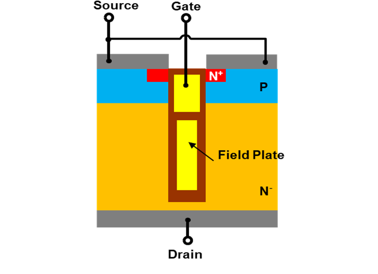
Structure and features
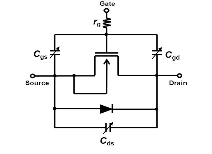
As shown in Fig. 1, our new generation low voltage MOSFET (12V-300V) has a Trench Field Plate (FP) under a gate electrode, and low drain-source on-resistance is achieved by increasing the concentration of the drift layer. Fig. 2 shows the schematic of SPICE model for FP-MOSFET which is developed by Toshiba. As a core MOSFET model, it is excellent in convergence and computation speed, and it adopts BSIM3v3 model which is implemented in most of circuit simulators of every EDA vendor. And the Field Plate shown in Fig. 1 producing additional capacitance components while relaxing electrolytic concentration. In order to express the non-linearity of capacitance characteristics due to this Field Plate structure, a non-linear capacitance Cgs/Cgd/Cds using optional function are constructed between each terminal.
MOSFET fitting accuracy
Fig. 3 shows the reproduction level (called "fitting accuracy") by comparing the actual measurement of ID-VGS characteristics and ID-VDS characteristics of our FP-MOSFET product TPH1R306PL with the simulation using the SPICE model. Our SPICE model for FP-MOSFET does not match the saturation characturistics in the high current region of ID-VGS characteristics commonly found in power MOSFET. On the other hand, it can be seen on Fig. 3 (a) and (b) that our SPICE model have higher reproducibility mainly on the reproducibility near the threshold voltage (Vth) and the reproducibility of the drain-source on-resistance (RDS (ON)) and the slope of the drain current ID in the ID-VDS characteristic.
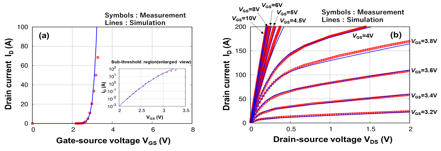
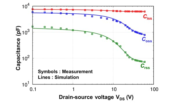
Figure 4 shows a comparison between actual measurement and simulation of the VDS dependencies on the Input capacitance (Ciss), Output capacitance (Coss) and Reverse transfer capacitance (Crss). The Trench Field Plate structure enables lower on-resistance by reducing the electric field concentration around the gate along with the enhancement of non-linearlity on the characteristics between gate capacitances and VDS. Toshiba SPICE model for FP-MOSFET reproduces the non-linear gate capacity property of the actual measurement with high accuracy by utilizing the non-linear capacitance combining several arbitrary functions as Cgs, Cgd, Cds.
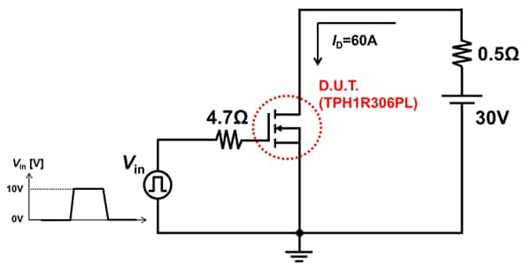
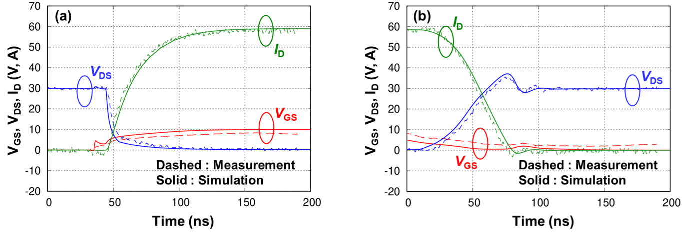
Transient characteristics (resistive load switching operation) fitting accuracy
Fig. 5 shows a resistive load switching circuit diagram using FP-MOSFET product, TPH1R306PL. And Fig. 6 (a) and (b) show the comparison between the actual measurement and the simulation for turn-on and turn-off characteristics using the resistive load switching circuit, respectively. As a result, it can be seen that the simulation waveform can reproduce the measured waveform with high accuracy for both turn-on and turn-off characteristic.
High accurate SPICE model (G2 model) to evaluate systems (300W isolated DC-DC converter)
The power conversion efficiency and the switching waveform of the MOSFET are compared by using the actual 300W isolated DC-DC converter reference design and the simulation circuit that applies the high accurate SPICE model (G2 model). Fig. 7 shows the appearance of the actual 300W isolated DC-DC converter and a schematic diagram of the simulation circuit.
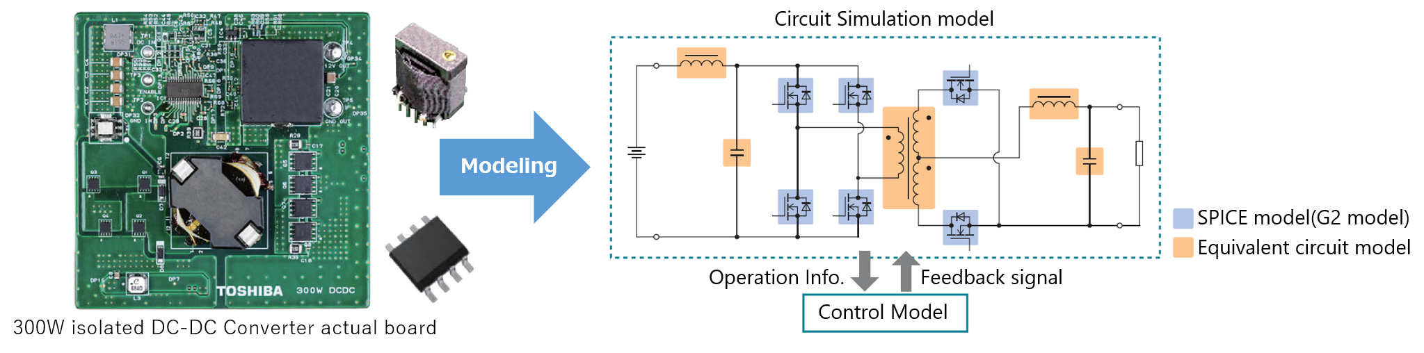
Fig. 8 shows the comparison of the load current dependency on the power conversion efficiency between actual measurement and simulation when TPN1200APL is mounted on the primary side of the DC-DC converter circuit and TPH2R408QM is mounted on the secondary side. It can be seen that the efficiency difference between measurment and simulation is 2% or less. This difference is mainly due to the factors not taken into account in this simulation circuit, such as loss of the controller and the temperature dependency on each component constituting the circuit.
Fig. 9 shows a simulation result of the loss calculated for the main components of a 300W isolated DC-DC converter. The total MOSFET loss on the primary and secondary sides at 25A output current accounts for approximately 43% of the total loss (the subtotal loss ratio of Pre_Side and Sec_Side in Fig. 9), and this ratio increases with the decrease of output current.

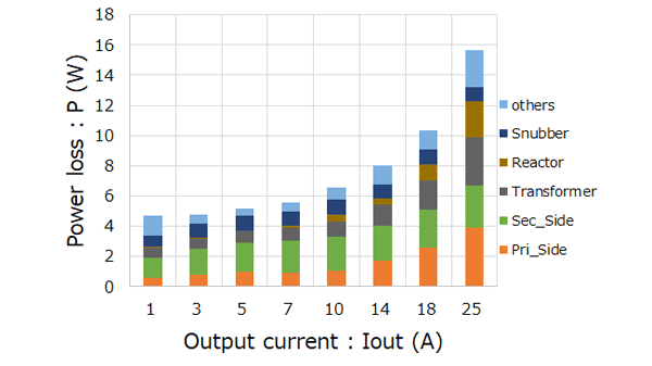
This result indicates that it is very important to reduce the loss on MOSFETs in order to improve the power conversion efficiency of the DC-DC converter. The detailed loss analysis during the switcing of the MOSFETs on the primary and/or secondary side is required for reduction of MOSFET loss, and the reproducibility of the switching waveform of the SPICE model is important.
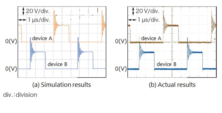
Fig. 10 shows a switching waveform comparison of TPH2R408QM used in the secondary side synchronous rectifier circuit of the DC-DC converter between actual measurement and simulation. According to this, a switching waveform simulated by G2 model that reflects the non-linearity of the capacitance characteristics with high accuracy is closely reproduced with the actual measurement can be obtained by simulation, therefore the quantitive MOSFET loss analysis is expected to be realized.
(Note) The high accuracy simulation circuit is developed uniquely for loss analysis.
Our high accurate SPICE model (G2 model) can reproduce the actual switching waveforms with high accuracy. The circuit verification by using high-accuracy simulation in advance of the actual production may reduce the double work for the circuit modification and help the development time shorten. Toshiba's high accurate SPICE model (G2 model) supports your circuit development and analysis effectively.