Gate-Driver IC for Automotive Three-Phase Brushless Motor: TB9084FTG
A gate-driver IC with the minimum functions required for automotive applications, with an emphasis on versatility. For all body-related systems, pumps, and motor generators that use three-phase brushless motors.
<Points of this product>
- Contributes to system design flexibility
- Contributes to ECU[1] size reduction by adopting a small package
The number of motors used within automotive equipment continues to increase, and the growth of three-phase brushless motors, which are relatively superior in terms of long life and quietness, is remarkable. Toshiba Electronic Devices & Storage Corporation ("Toshiba") is working to strengthen its product lineup to meet this demand, and the TB9084FTG shown here is part of that strengthening (Table 1).
Table 1. Our lineup of automotive gate-driver IC for three-phase brushless motor
| Part Number | Status | Package | GD | CP | MC SA |
GD for SR | SPI | Comment |
|---|---|---|---|---|---|---|---|---|
| TB9081FG | MP | LQFP64 | ○ (3phase) |
○ (3TBV) |
○ (3ch) |
○ (5ch) |
○ |
Full functionality for EPS. ASIL-D support. |
| TB9083FTG | MP | QFN48 | ○ (3phase) |
○ (3TBV) |
○ (3ch) |
○ (3ch) |
○ |
Cut down from TB9081. (e.g. the number of channel of GD for safety relay) ASIL-D support. |
| TB9084FTG | MP | QFN36 | ○ (3phase) |
○ (3TBV) |
○ (1ch) |
○ (1ch) |
○ |
Cut down from TB9083 for various application. (e.g. Deleted SR gate driver and diagnosis functionality, Reduced GD current capability) |
| TPD7212F | MP | QFN32 | ○ (3phase) |
○ (3TBV) |
- | - | - | Highly versatile device with minimum functionality. |
In the past, there was a large gap between "TPD7212F" (minimum necessary functions) and "TB9083FTG" (ASIL-D[2] capable functions) in terms of functions installed, but TB9084FTG will eliminate this gap and meet a wide variety of customer needs.
Minimum functions required for automotive equipment
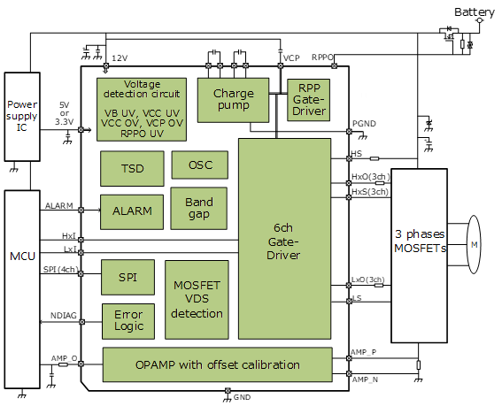
The TB9084FTG drives external Nch-MOSFETs that drive a three-phase brushless motor. Since a voltage is output to this gate, it is called a gate driver IC. It also has one more output pin channel to control an external Nch-MOSFET. It can be used for protection against battery reverse connection, as well as for power shutdown relay, etc. Regarding SPI communication, in addition to the function of reading abnormality detection flags, it has functions for setting thresholds between normal and abnormal states, as well as configuring reaction operations after detecting abnormal states, allowing it to accommodate various use cases. In addition, it has one channel of operational amplifiers to monitor the current flowing in the motor. This operational amplifier is equipped with a function to calibrate the input offset voltage, which is ±1mV under standard conditions[3] after this function is executed.

UV for Under Voltage, OV for Over voltage, TSD for Thermal Shut Down, OSC for Oscillator, RPP for Reverse Polarity Protection, SPI for Serial Peripheral Interface, OPAMP for OPerational AMPlifier, and MCU is abbreviation for Micro Controller Unit. In addition to driving three-phase brushless motors, it has the minimum functions required for automotive applications, detecting system abnormalities, and supporting protection.
TB9084FTG Product Value 1:
Contributes to system design flexibility
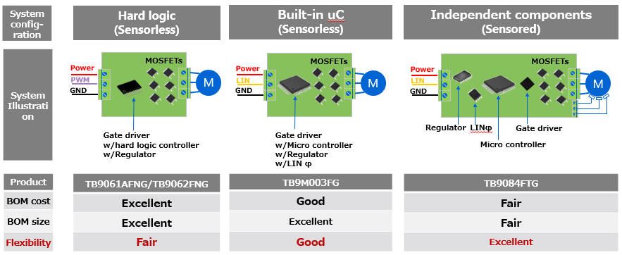
The TB9084FTG is designed to be mounted in an ECU that consists of a microcontroller, Nch-MOSFET, power supply IC, and communication PHY[4] as individual components (right side of Figure 2). Although this configuration has disadvantages in terms of total component size and cost, it is flexible enough to accommodate changes in system requirements, since only the relevant components need to be replaced when changes occur. On the other hand, there is a configuration in which motor control is performed by hard logic (left side of Figure 2). This configuration offers advantages in terms of total size and cost, however, it is limited in its ability to respond to changes in the environment surrounding motors. Another configuration is one in which motor control is performed by a microcontroller while its peripheral components are integrated into a single product (center of Figure 2). This configuration has the best balance of advantages/disadvantages. However, the microcontroller, which is often seen as a universal component, has a finite processing capacity, and when changes in system requirements exceed that capacity, changes tend to be large because functions other than the microcontroller are also renewed.

Toshiba is able to offer products for all of the three configurations described above and will provide optimal solutions for a wide variety of system requirements.
Please see the following pages for more information on the products listed in Figure 2.
TB9084FTG Product Value 2:
Contributes to ECU size reduction
Minimizing functions allows utilization of one of the small packages, the 6×6mm VQFN36, and contributes to equipment miniaturization. The package also has a wettable flank[5] structure, facilitating easy visual inspection to confirm the reliability of soldered joints.

The QFN package for this product is a wettable type, which improves mounting reliability and inspectability, in consideration of automotive applications. Also, by hiding the corner pins that have GND potential in the mold resin, the risk of malfunctions due to short failures between pins is reduced.
TB9084FTG main specifications
The power supply (VB, VCC) is intended for use in 12V battery systems and jump-start environments. The guaranteed chip temperature range is -40°C to 175°C, which corresponds to Grade 0 in the AEC-Q100[6]. As for the electrical characteristics of the gate driver, its output voltage is sufficient to drive an external Nch-MOSFET even with a low VB supply. Its current capability enables PWM[7] control at 20 kHz for a MOSFET with a gate input charge (Qg) of around 55 nC and an ID[8] equivalent to 50 A. The main specifications are shown below.
Please refer to the following page for our MOSFET that meets these characteristics.
Recommended MOSFET (TPH1R104PB)
ABSOLUTE MAXIMUM RATINGS (Excerpt)
| Spec # |
Item | Terminal | Symbol | Absolute maximum rating | Unit | Condition |
|---|---|---|---|---|---|---|
| 8.1 | Power supply | VB | Vb | -0.3~28 (DC) | V | 1V/s<Vb<8V/μs (Design value) |
| 8.2 | 28~40 (≦1s) | |||||
| 8.3 | VCP | Vcp | -0.3~60 (DC) | - | ||
| 8.4 | VCC | Vcc | -0.3~6 | 1V/s<Vcc<0.3V/μs (Design value) |
OPERATING VOLTAGE RANGES (Excerpt)
| Spec # |
Item | Terminal | Symbol | Operating voltage range | Unit | Condition |
|---|---|---|---|---|---|---|
| 9.1.1 | Input voltage | VB | Vb | 5.7~28 | V | DC |
| 9.1.2 | VCC | Vcc | 3.0~5.5 |
ELECTRICAL CHARACTERISTICS (Excerpt)
Vb=5.7 to 28V, Vcc=3.0 to 5.5V, Tj=-40 to 175°C unless otherwise specified.
| Spec # |
Item | Terminal | Symbol | Condition | Min | Typ. | Max | Unit |
|---|---|---|---|---|---|---|---|---|
| 9.3.1 | Charge pump output voltage |
VCP | Vcph1 | 5.7V≦Vb<7V load = -10µA~-13mA |
Vb+7.5 | Vb+9.3 | Vb+12.5 | V |
| 9.3.2 | Vcph2 | 7V≦Vb≦28V Iload = -10µA~-13mA |
Vb+9 | Vb+12 | Vb+14.5 | |||
| 9.4.5 | Gate driver output voltage for external MOSFET on high side |
HUO, HVO, HWO |
Voh1 | Voh1=H*O - H*S Iload=-100μA 7V≦Vb≦28V, H*S=0V |
7 | 10 | 12 | |
| 9.4.6 | Voh1_2 | Voh1_2=H*O - H*S Iload=-100μA 5.7V≦Vb<7V, H*S=0V |
Vcp-0.3 | - | Vcp | |||
| 9.4.7 | Vol1 | Vol1=H*O - H*S Iload=100μA |
0 | 0.2 | ||||
| 9.4.8 | Gate driver output voltage for external MOSFET on low side |
LUO, LVO, LWO |
Voh2 | Voh2=L*O - LS LS=0V Iload=-100μA |
6.7 | 11 | 12 | |
| 9.4.9 | Vol2 | Vol2=L*O - LS Iload=100μA LS=0V |
0 | - | 0.2 | |||
| 9.4.11 | Gate driver source output resistance |
HUO, HVO, HWO, LUO, LVO, LWO |
Rohh | HUI,HVI, HWI = VCC LUI, LVI, LWI = VCC Iload = -50mA |
- | 8.8 | 24 | Ω |
| 9.4.12 | Gate driver sink output resistance |
Rohl | HUI, HVI, HWI = 0V LUI, LVI, LWI = 0V Iload = 50mA |
3 | 6 |
The gate driver for high-side MOSFETs switches the output circuit configuration according to the VB voltage status. When the VB voltage is sufficient, a clamped voltage is output because of the sufficient charge pump voltage (Spec#9.4.5). When the VB voltage is not sufficient, the charge pump voltage is also low, so the charge pump voltage is output as it is (Spec#9.4.6).
Free lending of product evaluation board
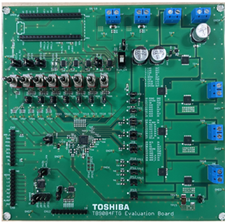
To enable customers to easily verify the characteristics of the TB9084FTG, we provide evaluation boards free of charge. Please contact our sales staff or our business partners at your service.

The size of the evaluation board is 150mm×160mm. This IC is mounted slightly left-bottom from the center. For customer convenience, switches, jumpers, and connectors are mounted as appropriate.
Toshiba is currently working to enhance a product lineup of ICs that control motors for automotive equipment. We will contribute to the electrification of automotive equipment and the improvement of comfort by introducing products to the market that optimize the functions and performance built into ICs to meet customers' needs.
Notes:
[1] Abbreviation for Electronic Control Unit, a device with electronic components mounted on a circuit board.
[2] ASIL: Automotive Safety Integrity Level, D: Grade D (highest rank from A to D)
[3] Ta=25℃, gain setting=15, input common mode voltage =0V、output load =0.5mA
[4] An IC responsible for the physical layer in the OSI reference model. Physical→PHY.
[5] The form of lead side of package. A terminal structure that allows automatic visual inspection (AVI) of installation on boards.
[6] Reliability testing and other standards for automotive ICs defined by the Automotive Electronics Council.
[7] PWM stands for Pulse Width Modulation, a method of controlling the power applied to a motor.
[8] ID is the current flowing in the drain (D) of a MOSFET.
Related information
Queries about purchasing, sampling and IC reliability
Stock Check & Purchase
require 3 characters or more.
* SmartMCD™ is a trademark of Toshiba Electronic Devices & Storage Corporation.
* Other company names, product names, and service names may be trademarks of their respective companies.


