- General Top
- SEMICONDUCTOR
- STORAGE
- COMPANY
-
My ToshibaSemicon
- Semiconductor Top
-
ApplicationsAutomotive
Body Electronics
xEV
In-Vehicle Infotainment
Advanced Driver-Assistance Systems (ADAS)
Chassis
IndustrialInfrastructure
BEMS/HEMS
Factory Automation
Commercial Equipment
Consumer/PersonalIoT Equipment
Healthcare
Wearable Device
Mobile
Computer Peripherals
-
ProductsAutomotive Devices
Discrete Semiconductor
Diodes
Transistors
Logic ICs
Analog Devices
- Automotive SmartMCD™ (Integreted SoC Conbining Microcontroller and Driver)
- Automotive Brushless Motor Driver ICs
- Automotive Brushed DC Motor Driver ICs
- Automotive Stepping Motor Driver ICs
- Automotive Driver ICs
- Automotive System Power Supplies ICs
- Automotive audio power amplifier ICs
- Automotive Network Communication
Digital Devices
Wireless Devices
※
 : Products list (parametric search)Power Semiconductors
SiC Power Devices
※
: Products list (parametric search)Isolators/Solid State RelaysPhotocouplers
Digital Isolators
Solid State Relays
Fiber Optic Transmitting Modules
※
: Products list (parametric search)MOSFETsIGBTs/IEGTsBipolar Transistors※
: Products list (parametric search)Diodes※
: Products list (parametric search)MicrocontrollersMotor Driver ICsIntelligent Power ICs※
: Products list (parametric search)Power Management ICsLinear ICs※
: Products list (parametric search)General Purpose Logic ICsLinear Image SensorsOther Product ICsOther Product ICs
※
: Products list (parametric search) -
Design & Development
Design & Development
Innovation Centre
At the Toshiba Innovation Centre we constantly strive to inspire you with our technologies and solutions. Discover how to place us at the heart of your innovations.
-
Knowledge
Knowledge
Highlighted Topics
Further Materials
Other
- Where To Buy


- Part Number & Keyword Search
- Cross Reference Search
- Parametric Search
- Stock Check & Purchase
This webpage doesn't work with Internet Explorer. Please use the latest version of Google Chrome, Microsoft Edge, Mozilla Firefox or Safari.
require 3 characters or more. Search for multiple part numbers fromhere.
The information presented in this cross reference is based on TOSHIBA's selection criteria and should be treated as a suggestion only. Please carefully review the latest versions of all relevant information on the TOSHIBA products, including without limitation data sheets and validate all operating parameters of the TOSHIBA products to ensure that the suggested TOSHIBA products are truly compatible with your design and application.Please note that this cross reference is based on TOSHIBA's estimate of compatibility with other manufacturers' products, based on other manufacturers' published data, at the time the data was collected.TOSHIBA is not responsible for any incorrect or incomplete information. Information is subject to change at any time without notice.
require 3 characters or more.
How to manage the power supply of mobile devices with high accuracy

In addition to being smaller, thinner, and lighter, user’s demand to power supply management of mobile devices which are becoming high functionality is increasingly severer. LDO regulators are often used when high accuracy power supply voltages are required. When selecting an LDO regulator, it cannot be judged only by the output voltage accuracy described in the data sheet. Characteristics such as ripple rejection ratio and load transient response must be checked. Toshiba's TCR5BM and TCR8BM series provide a stable power supply for mobile devices by devising circuit configurations to achieve high accuracy output voltages, while delivering low dropout voltages.
Load transient response and ripple rejection ratio
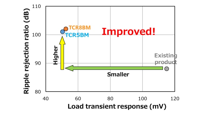
The load current connected to the output of the LDO regulator may increase or decrease suddenly. At this time, the output voltage may also fluctuate temporarily, and when the fluctuation is large, it may cause adverse effects such as malfunction or stop of the equipment. The load transient response is represented by the peak value of the fluctuation appearing in the output voltage for a stepwise change in the output current, indicating that the smaller the value, the more stable the voltage can be supplied.
The power supply line also has voltage fluctuations with various frequency components due to the operation of the various devices connected to the line. For power supply ICs, voltage fluctuations superimposed on the input power line become a problem. These fluctuations are called the ripple voltage, and the LDO regulator is characterized by suppressing the propagation of the ripple voltage superimposed on the input voltage to the output side. The ripple rejection ratio is the value that represents this characteristic.
TCR5BM/8BM series has improved load transient response and ripple rejection ratio. It has excellent response performance against sudden current changes and provides stable constant voltage operation with minimal voltage fluctuation. In addition, excellent ripple rejection ratio is achieved in a wide frequency range by optimizing the gain of each frequency band, etc.
With these features, TCR5BM/8BM can minimize the effects of load current fluctuations and input noise on the output, and provides a stable output voltage as the load side power supply.
Refer to following link for the details of load transient response and ripple rejection ratio.
Dropout voltage characteristics

TCR5BM/8BM series also improves dropout voltages, in addition to load transient response and ripple rejection ratio.
A voltage higher than the input voltage is applied to the bias terminal separated from the input terminal, and drives the gate of the built-in output MOSFET so that the difference between the input voltage and the output voltage can be reduced.
The LDO regulator is buck-type, so normally set the input voltage higher than the output. Since the dropout voltage is also a limit value at which the drop in the input voltage does not affect the output voltage, it can be said that the output voltage is configured to be less susceptible to input fluctuations.
The power consumption of the regulator itself is the difference between the input and output voltages multiplied by the output current. Reducing the difference between the input and output voltages also reduces power consumption that causes heat generation. This can reduce or eliminate heat generation measures such as securing space and attaching a heat sink, and helps reduce the size and weight of the mounting set.
Refer to following link for the details of dropout voltage and power consumption.
Recommended product list
Product Number |
|
|
|||
|---|---|---|---|---|---|
Data sheet |
|||||
Package name, dimensions (mm), outline drawing |
DFN5B
|
DFN5B
|
|||
Operating range |
Output voltage (V) |
0.8 to 3.6 |
0.8 to 3.6 |
||
Output current (A) |
0 to 0.5 |
0 to 0.8 |
|||
Electrical Characteristics |
Bias current (μA) |
Max |
@IOUT=0 mA, VBIAS terminal current |
36 |
36 |
Max |
@IOUT=0 mA, VIN terminal current |
6 |
6 |
||
Dropout voltage (mV) |
Max |
@IOUT=500 mA, VOUT=1.1 V, TCR5BM |
140 |
- |
|
Max |
@IOUT=800 mA, VOUT=1.1 V, TCR8BM |
- |
245 |
||
Ripple compressibility (dB) |
Typ. |
@IOUT=10 mA, f=1 kHz, VIN Ripple=200 mVp-p, VOUT=0.8 V |
98 |
98 |
|
Load transient response (mV) |
Typ. |
@IOUT=1 mA → |
-100 |
-100 |
|
Typ. |
@IOUT = Max output current → |
100 |
100 |
||