
- General Top
- SEMICONDUCTOR
- STORAGE
- COMPANY
-
My ToshibaSemicon
- Semiconductor Top
-
ApplicationsAutomotive
Body Electronics
xEV
In-Vehicle Infotainment
Advanced Driver-Assistance Systems (ADAS)
Chassis
IndustrialInfrastructure
BEMS/HEMS
Factory Automation
Commercial Equipment
Consumer/PersonalIoT Equipment
Healthcare
Wearable Device
Mobile
Computer Peripherals
-
ProductsAutomotive Devices
Discrete Semiconductor
Diodes
Transistors
Logic ICs
Analog Devices
Digital Devices
Wireless Devices
※
 : Products list (parametric search)Power Semiconductors
SiC Power Devices
※
: Products list (parametric search)Isolators/Solid State RelaysPhotocouplers
Digital Isolators
Solid State Relays
Fiber Optic Transmitting Modules
※
: Products list (parametric search)MOSFETsIGBTs/IEGTsBipolar Transistors※
: Products list (parametric search)Diodes※
: Products list (parametric search)MicrocontrollersMotor Driver ICsIntelligent Power ICs※
: Products list (parametric search)Power Management ICsLinear ICs※
: Products list (parametric search)General Purpose Logic ICsLinear Image SensorsOther Product ICsOther Product ICs
※
: Products list (parametric search) -
Design & Development
Design & Development
Innovation Centre
At the Toshiba Innovation Centre we constantly strive to inspire you with our technologies and solutions. Discover how to place us at the heart of your innovations.
-
Knowledge
Knowledge
Highlighted Topics
Further Materials
Other
- Where To Buy


- Part Number & Keyword Search
- Cross Reference Search
- Parametric Search
- Stock Check & Purchase
This webpage doesn't work with Internet Explorer. Please use the latest version of Google Chrome, Microsoft Edge, Mozilla Firefox or Safari.
require 3 characters or more. Search for multiple part numbers fromhere.
The information presented in this cross reference is based on TOSHIBA's selection criteria and should be treated as a suggestion only. Please carefully review the latest versions of all relevant information on the TOSHIBA products, including without limitation data sheets and validate all operating parameters of the TOSHIBA products to ensure that the suggested TOSHIBA products are truly compatible with your design and application.Please note that this cross reference is based on TOSHIBA's estimate of compatibility with other manufacturers' products, based on other manufacturers' published data, at the time the data was collected.TOSHIBA is not responsible for any incorrect or incomplete information. Information is subject to change at any time without notice.
require 3 characters or more.
Combatting Heat Dissipation Issues as Higher Density Power Systems are Deployed
Rapidly escalating power densities in semiconductor devices are being expected in order to provide consumers with sleeker, more attractive electronic products that possess greater functionality while also supporting longer periods between recharges. As a result, the specification of key elements of the power system, such as MOSFETs, must be given substantial consideration, so that well-reasoned procurement decisions are made. As higher power density devices are employed, the issue of coping with the increased generation of heat energy needs to be tackled. This means that effective thermal management now, more than ever, is vital to modern power system design - and this should clearly start at the component level.
The cooling mechanisms generally used in electronics hardware to dissipate heat energy (heatsinks, fans, heatpipes, etc.) add significantly to the cost, size and complexity of the system. These are all things that engineers want to avoid as much as possible, as they have to deal with an array of different constraints - in terms of available board space, time to market and the unit cost of the end product. Moving to higher power densities achieves absolutely nothing if the disadvantages end up outweighing the benefits. Cooling fans, it should be noted, prove particularly inconvenient, as not only do they expand the size of the enclosure needed, they also contribute to the system’s power budget. Furthermore, inclusion of fans prevents sealing of the enclosure (leaving the electronics inside potentially exposed to dust or moisture ingress) and, as they have moving parts involved, operational failures can occur.
Engineers simply cannot afford to ignore the heat dissipation issue, but a new approached is needed. They have always had the unenviable task of balancing power efficiency characteristics and switching speeds. By minimising the MOSFET’s gate charge (Qg) it has been possible to achieve higher switching speeds, but this has meant greater power losses - as the on-state resistance (RDS(ON)) has risen. In contrast efforts to curb the RDS(ON) to mitigate power losses have led to poorer switching performance being witnessed. It isn’t possible, with any given device, to make enhancements to one of these parameters without having the other one suffer to some degree. This is why MOSFET datasheets will normally reference both these parameters together in the form of the following figure of merit:
RDS(ON) x Qg
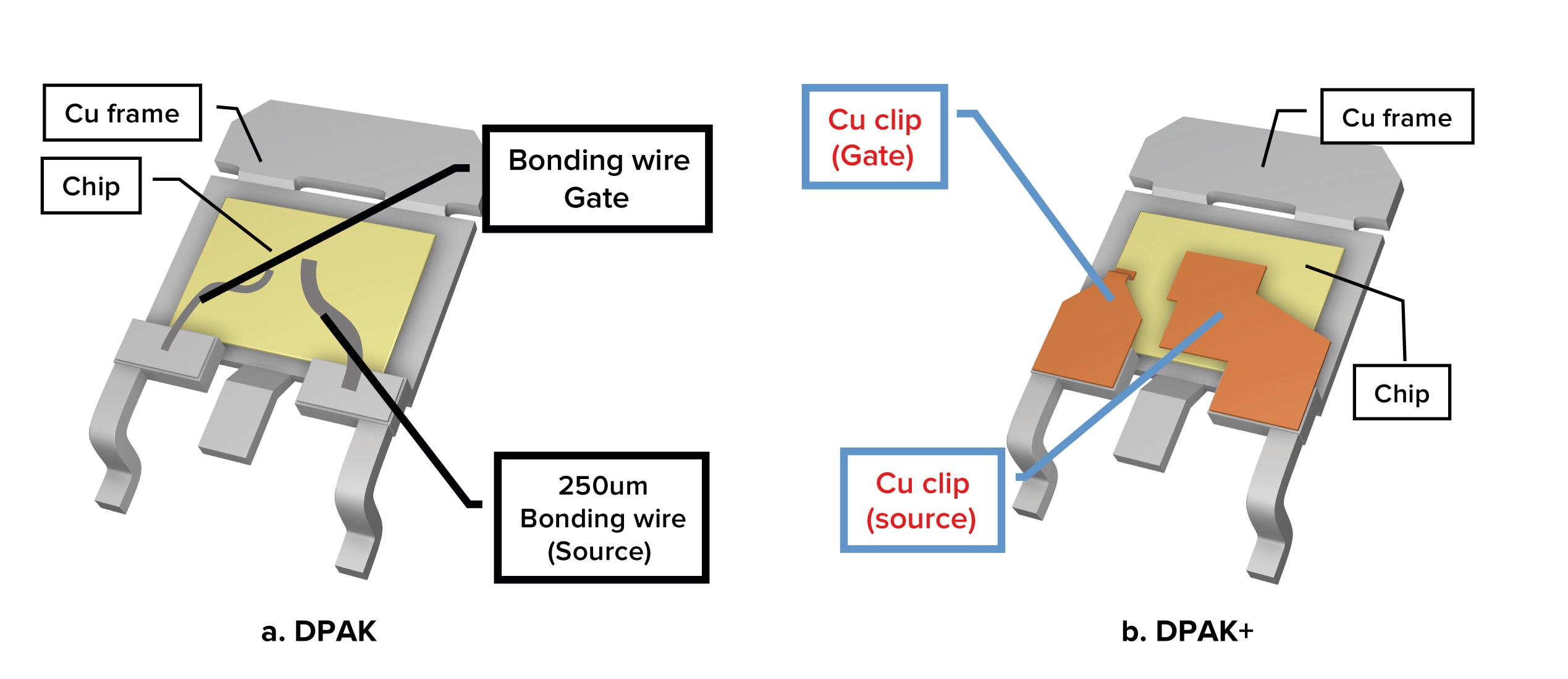
Unable to break this loop, engineers need ground-breaking innovation from power IC manufacturers, so that better MOSFET figure of merits are forthcoming. The introduction of new generations of semiconductor process technologies, along with the implementation of better realised trench arrangements, are set to enable power conversion efficiencies to be boosted. This means that the desired improvements to MOSFET figure of merit values can be brought about. At the same time significant advances in power IC packaging design are taking place. Over the years traditional package formats have been supplanted - first through-hole gave way to ball grid arrays, now thermal pads are being replaced by copper clips. The subsequent thermal conductivity improvements are enabling the heat energy generated to be removed from devices in a much more effective manner (carrying heat away from both the topside and the underside of the die).
To find out more about Toshiba’s latest innovations in MOSFET design and how these are facilitating systems with higher power densities, download the following white paper: