
- General Top
- SEMICONDUCTOR
- STORAGE
- COMPANY
-
My ToshibaSemicon
- Semiconductor Top
-
ApplicationsAutomotive
Body Electronics
xEV
In-Vehicle Infotainment
Advanced Driver-Assistance Systems (ADAS)
Chassis
IndustrialInfrastructure
BEMS/HEMS
Factory Automation
Commercial Equipment
Consumer/PersonalIoT Equipment
Healthcare
Wearable Device
Mobile
Computer Peripherals
-
ProductsAutomotive Devices
Discrete Semiconductor
Diodes
Transistors
Logic ICs
Analog Devices
- Automotive SmartMCD™ (Integreted SoC Conbining Microcontroller and Driver)
- Automotive Brushless Motor Driver ICs
- Automotive Brushed DC Motor Driver ICs
- Automotive Stepping Motor Driver ICs
- Automotive Driver ICs
- Automotive System Power Supplies ICs
- Automotive audio power amplifier ICs
- Automotive Network Communication
Digital Devices
Wireless Devices
※
 : Products list (parametric search)Power Semiconductors
SiC Power Devices
※
: Products list (parametric search)Isolators/Solid State RelaysPhotocouplers
Digital Isolators
Solid State Relays
Fiber Optic Transmitting Modules
※
: Products list (parametric search)MOSFETsIGBTs/IEGTsBipolar Transistors※
: Products list (parametric search)Diodes※
: Products list (parametric search)MicrocontrollersMotor Driver ICsIntelligent Power ICs※
: Products list (parametric search)Power Management ICsLinear ICs※
: Products list (parametric search)General Purpose Logic ICsLinear Image SensorsOther Product ICsOther Product ICs
※
: Products list (parametric search) -
Design & Development
Design & Development
Innovation Centre
At the Toshiba Innovation Centre we constantly strive to inspire you with our technologies and solutions. Discover how to place us at the heart of your innovations.
-
Knowledge
Knowledge
Highlighted Topics
Further Materials
Other
- Where To Buy


- Part Number & Keyword Search
- Cross Reference Search
- Parametric Search
- Stock Check & Purchase
This webpage doesn't work with Internet Explorer. Please use the latest version of Google Chrome, Microsoft Edge, Mozilla Firefox or Safari.
require 3 characters or more. Search for multiple part numbers fromhere.
The information presented in this cross reference is based on TOSHIBA's selection criteria and should be treated as a suggestion only. Please carefully review the latest versions of all relevant information on the TOSHIBA products, including without limitation data sheets and validate all operating parameters of the TOSHIBA products to ensure that the suggested TOSHIBA products are truly compatible with your design and application.Please note that this cross reference is based on TOSHIBA's estimate of compatibility with other manufacturers' products, based on other manufacturers' published data, at the time the data was collected.TOSHIBA is not responsible for any incorrect or incomplete information. Information is subject to change at any time without notice.
require 3 characters or more.
Thermal Management Implications of Advances in Packaging & Silicon Technologies for Power Semiconductor Devices
The heat energy that is present in power ICs, such as MOSFETs, not only impacts on these devices’ operational performance, it also has the potential to impinge heavily on system reliability, increasing the risk of failure and shortening operational lifespan. It has a detrimental effect on the running costs involved too - as power adaptors that exhibit poor conversion efficiency characteristics will need to draw more current from the main supply, thus adding to the size of the user’s utility bills. Engineers simply cannot afford to ignore the heat dissipation issue.
The importance of implementing adequate thermal management resources is increasing as higher density power technology is incorporated into system designs, but this also has repercussions. It leads to the utilising of value board space, the increasing of bill-of-materials costs and the raising overall system complexity. Furthermore, if the cooling mechanism is electro-mechanical in nature (such as a fan), it can also raise the power budget substantially.
OEMs are seeking out more effective ways to ensure that inside their products the amount of energy converted into heat is kept to a minimum. This will mean that such products can be placed into enclosures with smaller form factors (that are more attractive to consumers) and have higher power ratings that will thereby facilitate support for a greater breadth of features and functionality (which will mean that their products have the edge of those of their rivals). More has to be done at the component level to address OEM demands, but unfortunately things are in reality not that simple.
Keeping both power efficiency and switching speeds at acceptable levels has traditionally been a difficult (and at times frustrating) balancing act. Trying to maintain a low on-state resistance (RDS(ON)) so that conduction performance is enhanced has normally meant compromising on the MOSFETs switching characteristics. Conversely, optimising the device to minimise gate charge (Qg) has allowed higher switching speeds to be benefited from, but has also heightened the RDS(ON) and increased power losses once again - the trade-off between these two parameters being described via the device’s figure of merit (RDS(ON) x Qg).
The progress being made in power semiconductor fabrication is now bringing about marked improvements in power conversion efficiencies. This means that less heat is generated. To complement this, the implementation of more sophisticated IC packaging is expediting the heat dissipation process. What is therefore needed is a two-pronged attack. From a silicon perspective, innovation is leading to improvements in power conversion efficiency and mitigating heat generation issues. At the same time more advanced packaging technology design is enabling heat to be removed from the system.
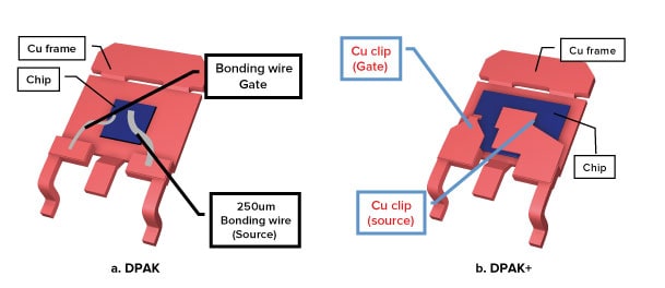
Toshiba’s latest generation UMOS are housed in DPAK+ packages which have the same dimensions and outline as the conventional DPAK format, but utilise copper clips (rather than aluminium bondwires) to connect the gate and source pins directly to the metallised electrodes on the die in order to combat power losses.
To learn more about Toshiba’s innovations in power IC design, download the following white paper: