- General Top
- SEMICONDUCTOR
- STORAGE
- COMPANY
-
My ToshibaSemicon
- Semiconductor Top
-
ApplicationsAutomotive
Body Electronics
xEV
In-Vehicle Infotainment
Advanced Driver-Assistance Systems (ADAS)
Chassis
IndustrialInfrastructure
BEMS/HEMS
Factory Automation
Commercial Equipment
Consumer/PersonalIoT Equipment
Healthcare
Wearable Device
Mobile
Computer Peripherals
-
ProductsAutomotive Devices
Discrete Semiconductor
Diodes
Transistors
Logic ICs
Analog Devices
- Automotive SmartMCD™ (Integreted SoC Conbining Microcontroller and Driver)
- Automotive Brushless Motor Driver ICs
- Automotive Brushed DC Motor Driver ICs
- Automotive Stepping Motor Driver ICs
- Automotive Driver ICs
- Automotive System Power Supplies ICs
- Automotive audio power amplifier ICs
- Automotive Network Communication
Digital Devices
Wireless Devices
※
: Products list (parametric search)
Power SemiconductorsSiC Power Devices
※
: Products list (parametric search)
Isolators/Solid State RelaysPhotocouplers
Digital Isolators
Solid State Relays
Fiber Optic Transmitting Modules
※
: Products list (parametric search)
MOSFETsIGBTs/IEGTsBipolar Transistors※
: Products list (parametric search)
Diodes※
: Products list (parametric search)
MicrocontrollersMotor Driver ICsIntelligent Power ICs※
: Products list (parametric search)
Power Management ICsLinear ICs※
: Products list (parametric search)
General Purpose Logic ICsLinear Image SensorsOther Product ICsOther Product ICs
※
: Products list (parametric search)
-
Design & Development
Design & Development
Innovation Centre
At the Toshiba Innovation Centre we constantly strive to inspire you with our technologies and solutions. Discover how to place us at the heart of your innovations.
-
Knowledge
Knowledge
Highlighted Topics
Further Materials
Other
- Where To Buy
- Part Number & Keyword Search
- Cross Reference Search
- Parametric Search
- Stock Check & Purchase
This webpage doesn't work with Internet Explorer. Please use the latest version of Google Chrome, Microsoft Edge, Mozilla Firefox or Safari.
require 3 characters or more. Search for multiple part numbers fromhere.
The information presented in this cross reference is based on TOSHIBA's selection criteria and should be treated as a suggestion only. Please carefully review the latest versions of all relevant information on the TOSHIBA products, including without limitation data sheets and validate all operating parameters of the TOSHIBA products to ensure that the suggested TOSHIBA products are truly compatible with your design and application.Please note that this cross reference is based on TOSHIBA's estimate of compatibility with other manufacturers' products, based on other manufacturers' published data, at the time the data was collected.TOSHIBA is not responsible for any incorrect or incomplete information. Information is subject to change at any time without notice.
require 3 characters or more.
How do MOSFET current and thermal limitations interact?

Power MOSFETs are popular switching elements in many modern power devices. As engineers try to squeeze ever more performance and efficiency from each design, then MOSFETs are pushed to their limit. However, there is obviously a limit to each device's capability, yet there is no single means to define this limitation as it depends on a number of factors that interact.
Generally speaking, MOSFETs with lower on-resistance (RON) are able to operate with higher currents. Devices exist with RON values lower than 1mW that can theoretically operate with currents up to 500A in a small 5mm x 6mm package. However, this is not realistic in practice as other parametric limits will inevitably be exceeded.
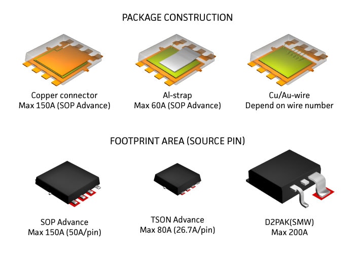
Toshiba MOSFET datasheets show the lowest (e.g. worst case) of several limitations, each of which is calculated or measured. Some of these datasheets show the silicon limitation as well as the lowest limitation, which always defines the limit for the device. For low resistance MOSFETs, the current limitation will mainly depend on the device package.
Any design incorporating MOSFETs is limited by temperature. Temperature depends on two factors; the ability to radiate heat and the on-resistance, which is proportional to heat generated. It does not depend on the drain current (ID).
Other topics for consideration include the carrier density, which puts a limit on ID to ensure that the MOSFET only operates in the linear region, and avalanche mode. Although avalanche mode does not apply to every MOSFET, for some the avalanche current can flow through an equivalent transistor formed by the diode-MOSFET combination. This current, if unchecked, can damage the MOSFET.
When comparing maximum ID values between Toshiba and other suppliers, engineers must ensure a good and valid comparison to be able to select the most appropriate device. Only through understanding the operation of the MOSFET electrically and thermally and applying the appropriate limits can this comparison be made.
Toshiba has produced a white paper with example calculations on this subject. To download your copy, please click here:


