
- General Top
- SEMICONDUCTOR
- STORAGE
- COMPANY
-
My ToshibaSemicon
- Semiconductor Top
-
ApplicationsAutomotive
Body Electronics
xEV
In-Vehicle Infotainment
Advanced Driver-Assistance Systems (ADAS)
Chassis
IndustrialInfrastructure
BEMS/HEMS
Factory Automation
Commercial Equipment
Consumer/PersonalIoT Equipment
Healthcare
Wearable Device
Mobile
Computer Peripherals
-
ProductsAutomotive Devices
Discrete Semiconductor
Diodes
Transistors
Logic ICs
Analog Devices
- Automotive SmartMCD™ (Integreted SoC Conbining Microcontroller and Driver)
- Automotive Brushless Motor Driver ICs
- Automotive Brushed DC Motor Driver ICs
- Automotive Stepping Motor Driver ICs
- Automotive Driver ICs
- Automotive System Power Supplies ICs
- Automotive audio power amplifier ICs
- Automotive Network Communication
Digital Devices
Wireless Devices
※
 : Products list (parametric search)Power Semiconductors
SiC Power Devices
※
: Products list (parametric search)Isolators/Solid State RelaysPhotocouplers
Digital Isolators
Solid State Relays
Fiber Optic Transmitting Modules
※
: Products list (parametric search)MOSFETsIGBTs/IEGTsBipolar Transistors※
: Products list (parametric search)Diodes※
: Products list (parametric search)MicrocontrollersMotor Driver ICsIntelligent Power ICs※
: Products list (parametric search)Power Management ICsLinear ICs※
: Products list (parametric search)General Purpose Logic ICsLinear Image SensorsOther Product ICsOther Product ICs
※
: Products list (parametric search) -
Design & Development
Design & Development
Innovation Centre
At the Toshiba Innovation Centre we constantly strive to inspire you with our technologies and solutions. Discover how to place us at the heart of your innovations.
-
Knowledge
Knowledge
Highlighted Topics
Further Materials
Other
- Where To Buy


- Part Number & Keyword Search
- Cross Reference Search
- Parametric Search
- Stock Check & Purchase
This webpage doesn't work with Internet Explorer. Please use the latest version of Google Chrome, Microsoft Edge, Mozilla Firefox or Safari.
require 3 characters or more. Search for multiple part numbers fromhere.
The information presented in this cross reference is based on TOSHIBA's selection criteria and should be treated as a suggestion only. Please carefully review the latest versions of all relevant information on the TOSHIBA products, including without limitation data sheets and validate all operating parameters of the TOSHIBA products to ensure that the suggested TOSHIBA products are truly compatible with your design and application.Please note that this cross reference is based on TOSHIBA's estimate of compatibility with other manufacturers' products, based on other manufacturers' published data, at the time the data was collected.TOSHIBA is not responsible for any incorrect or incomplete information. Information is subject to change at any time without notice.
require 3 characters or more.
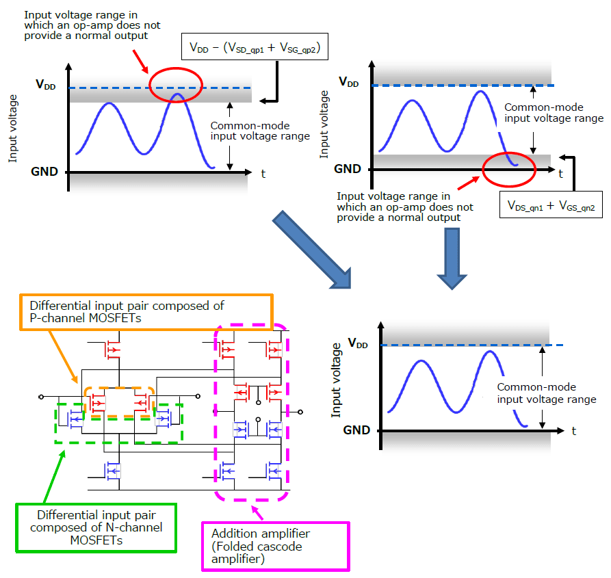
What is the common-mode input voltage (CMVIN) of an op-amp?
The common-mode input voltage (CMVIN) is defined in the electrical characteristics of the operational amplifier datasheet. This characteristic is input voltage that satisfies the electrical characteristics (CMRR, etc.) of the data sheet when the same signal is applied to the IN(+) and IN(-) terminals.
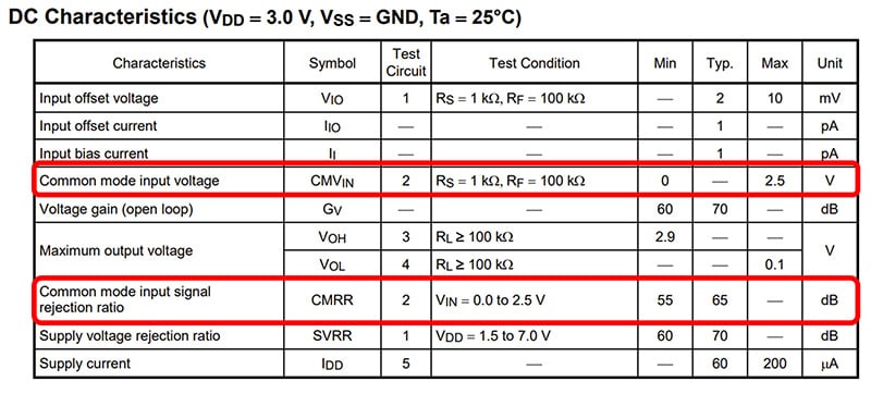
You might consider that common-mode signals are never applied to an op-amp. However, op-amps are commonly used with negative feedback, which results in the IN(+) and IN(-) terminals being virtually short-circuited. This is equivalent to applying common-mode signals (or signals with little difference in voltage) to the op-amp.
If the input signals of an op-amp are outside the specified common-mode input voltage range, the gain of the differential amplifier decreases, resulting in a distortion of the output signal. If the input voltage is even higher and exceeds the maximum rated differential input voltage, the device might deteriorate or be permanently damage.
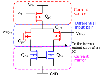
The equivalent input circuit of a typical op-amp consists of a differential input pair, a current source, and a current mirror (active load) as shown in Fig. 1. The current source established by the reference bias (VB1) determines the amount of current that flows to the differential input pair. Because of the current mirror circuit, the differential input pair basically provides Qn1 and Qn2 with the same current. As a result, VDS_qn2 is transferred to the output stage of the op-amp.
Suppose that VIN(+) and VIN(-) have dropped by ΔV. This causes the source-gate voltage (VSG) of Qp2 and Qp3 to increase, which in turn causes their drain current to increase. Since the current source provides more current, the drain-source voltage of Qp1 (VDS_qp1) also increases. As a result, the source-gate voltage (VSG) of Qp2 and Qp3 decreases back to the previous level.
Therefore, the output of an op-amp remains unchanged when common-mode signals are applied to its differential input pair.
The assumption of the above operations is that the MOSFETs are in the saturation region.
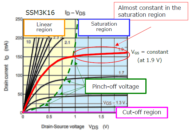
Next, let's consider the conditions under which the MOSFET enters the saturation region. Fig. 2 shows the I D-VDS curve of an N-channel MOSFET (SSM3K16). The drain current remains almost constant (ΔV/ΔI = high impedance) over the drain-source voltage (VDS) range in the saturation region. The following relationship must be satisfied in order for the MOSFET to operate in the saturation region, where Vth is the gate-source voltage (VGS) at which the drain current begins to flow.
VDS > VGS - Vth (1)
Here, we write an equation for VIN(+) with respect to GND to determine its minimum value, VIN(+)_min.
VIN(+) = VGS_qn1 + VSD_qp2 – VSG_qp2 (2)
At VIN(+)_min, the source-drain voltage of Qp2 decreases to a level called the pinch-off voltage at which Qp2 is about to transition from the saturation region to the linear region. Let this voltage be VSD_qp2_min and the threshold voltage of Qp2 at which the drain current begins to flow be Vth_qp2. Then, the following equation is obtained from Equation 1 that represents the saturation condition:
VSD_qp2_min = VSG_qp2 – Vth_Qp2 (3)
Substituting Equation 2 into Equation 3 gives:
VIN(+)_min = VGS_qn1 – Vth_qp2 (4)
Up until this point, we have regarded MOSFETs as three-terminal devices. In actuality, however, there is one more terminal called the back gate. (In the case of typical discrete MOSFETs, the back gate is internally connected to the source terminal.)
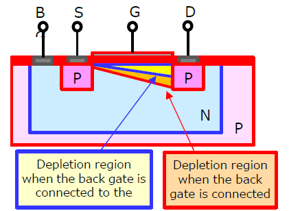
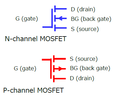
In the case of a P-channel MOSFET, when the back gate has higher voltage than the source, the depletion region expands, causing Vth to become higher. Therefore, the value of Vth in Equation 4 becomes higher when the back gates of Qp2 and Qp3 are connected to VDD. In addition, VIN(+)_min can be reduced to zero by reducing the pinch-off voltage (i.e., VGS_qn1 in Equation 4) through process optimization.
Next, we write an equation for VIN(+) with respect to VDD to determine its maximum value, VIN(+)_max.
VIN(+) = VDD – VSD_qp1 – VSG_qp2 (5)
When VIN(+) is applied, the source-drain voltage of Qp2 (VSD_qp2) increases, causing VSD_qp1 to reach the minimum saturation voltage (VSD_qp1_min). If VSD_qp2 increases further, Qp1 enters the linear region, causing the drain current and the gain to decrease.
Therefore, op-amps with a differential input pair composed of P-channel MOSFETs can be used with an input voltage (common-mode input voltage) between GND and VDD – (VSD_qp1 + VSG_qp2) whereas those with a differential input pair composed of N-channel MOSFETs can be used with an input voltage between (VDS_qn1 + VGS_qn2) and VDD.
In contrast to these types of op-amps, the input differential stage of a rail-to-rail op-amp consists of an N-channel MOSFET pair and a P-channel MOSFET pair connected in parallel. The common-mode input voltage range of the rail-to-rail op-amp extends across almost the entire range from GND to VDD.
Related Links
The following documents also contain related information:

