- General Top
- SEMICONDUCTOR
- STORAGE
- COMPANY
-
My ToshibaSemicon
- Semiconductor Top
-
ApplicationsAutomotive
Body Electronics
xEV
In-Vehicle Infotainment
Advanced Driver-Assistance Systems (ADAS)
Chassis
IndustrialInfrastructure
BEMS/HEMS
Factory Automation
Commercial Equipment
Consumer/PersonalIoT Equipment
Healthcare
Wearable Device
Mobile
Computer Peripherals
-
ProductsAutomotive Devices
Discrete Semiconductor
Diodes
Transistors
Logic ICs
Analog Devices
- Automotive SmartMCD™ (Integreted SoC Conbining Microcontroller and Driver)
- Automotive Brushless Motor Driver ICs
- Automotive Brushed DC Motor Driver ICs
- Automotive Stepping Motor Driver ICs
- Automotive Driver ICs
- Automotive System Power Supplies ICs
- Automotive audio power amplifier ICs
- Automotive Network Communication
Digital Devices
Wireless Devices
※
 : Products list (parametric search)Power Semiconductors
SiC Power Devices
※
: Products list (parametric search)Isolators/Solid State RelaysPhotocouplers
Digital Isolators
Solid State Relays
Fiber Optic Transmitting Modules
※
: Products list (parametric search)MOSFETsIGBTs/IEGTsBipolar Transistors※
: Products list (parametric search)Diodes※
: Products list (parametric search)MicrocontrollersMotor Driver ICsIntelligent Power ICs※
: Products list (parametric search)Power Management ICsLinear ICs※
: Products list (parametric search)General Purpose Logic ICsLinear Image SensorsOther Product ICsOther Product ICs
※
: Products list (parametric search) -
Design & Development
Design & Development
Innovation Centre
At the Toshiba Innovation Centre we constantly strive to inspire you with our technologies and solutions. Discover how to place us at the heart of your innovations.
-
Knowledge
Knowledge
Highlighted Topics
Further Materials
Other
- Where To Buy


- Part Number & Keyword Search
- Cross Reference Search
- Parametric Search
- Stock Check & Purchase
This webpage doesn't work with Internet Explorer. Please use the latest version of Google Chrome, Microsoft Edge, Mozilla Firefox or Safari.
require 3 characters or more. Search for multiple part numbers fromhere.
The information presented in this cross reference is based on TOSHIBA's selection criteria and should be treated as a suggestion only. Please carefully review the latest versions of all relevant information on the TOSHIBA products, including without limitation data sheets and validate all operating parameters of the TOSHIBA products to ensure that the suggested TOSHIBA products are truly compatible with your design and application.Please note that this cross reference is based on TOSHIBA's estimate of compatibility with other manufacturers' products, based on other manufacturers' published data, at the time the data was collected.TOSHIBA is not responsible for any incorrect or incomplete information. Information is subject to change at any time without notice.
require 3 characters or more.
What is the difference between the bus switch type and the buffer type of the voltage-level transformation IC (level shifter)?
The bus switch type uses MOSFETs as switches and performs voltage level shifting with external pull-up resistors. Since it is just a switch, it has no current drive capability. On the other hand, the buffer type outputs from the CMOS structure circuit and level shifts. Therefore, it has a product-specific drive capability, and the output is a digital signal.
Bus Switch Type Voltage translation IC (Level Shifter)
The bus switch type product (TC7SPB9306TU) can perform voltage level shift by switching on/off and using pull-up resistors. The OE pin is a control input that switches on/off.
With the connection shown in Fig. 1, we will explain the operation using an example of the waveform that is output from the right side (Input B) when an input signal is input from the left side (Input A).
The input/output transfer operation is divided into two operations, depending on the input voltage level, using VOHU (input level up characteristic) specified in the product data sheet (Table- 1) as a threshold.
0V to VOHU : The internal switch is on and transfers a signal from A to B without changing its voltage.
VOHU or higher: The internal switch is off. The external pull-up resistor on the VCCB side pulls up the input voltage to the VCCB level.
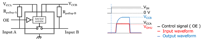
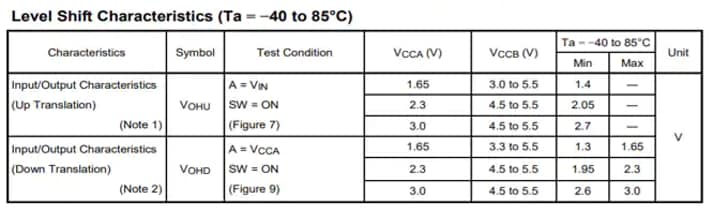
Table-1 VOHU and VOHD characteristics shown in the datasheet (TC7SPB9306TU)
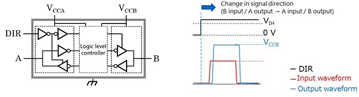
Buffer-type voltage-translation IC (level shifter)
Buffer type products output from the CMOS structure circuit and level shift. Therefore, it has a product-specific drive capability, and the output is a digital signal (Fig. 2). For specific values of drive capability, refer to the output current described in the operating range of the datasheet.
Related Links
The following documents also contain related information.