- General Top
- SEMICONDUCTOR
- STORAGE
- COMPANY
-
My ToshibaSemicon
- Semiconductor Top
-
ApplicationsAutomotive
Body Electronics
xEV
In-Vehicle Infotainment
Advanced Driver-Assistance Systems (ADAS)
Chassis
IndustrialInfrastructure
BEMS/HEMS
Factory Automation
Commercial Equipment
Consumer/PersonalIoT Equipment
Healthcare
Wearable Device
Mobile
Computer Peripherals
-
ProductsAutomotive Devices
Discrete Semiconductor
Diodes
Transistors
Logic ICs
Analog Devices
- Automotive SmartMCD™ (Integreted SoC Conbining Microcontroller and Driver)
- Automotive Brushless Motor Driver ICs
- Automotive Brushed DC Motor Driver ICs
- Automotive Stepping Motor Driver ICs
- Automotive Driver ICs
- Automotive System Power Supplies ICs
- Automotive audio power amplifier ICs
- Automotive Network Communication
Digital Devices
Wireless Devices
※
 : Products list (parametric search)Power Semiconductors
SiC Power Devices
※
: Products list (parametric search)Isolators/Solid State RelaysPhotocouplers
Digital Isolators
Solid State Relays
Fiber Optic Transmitting Modules
※
: Products list (parametric search)MOSFETsIGBTs/IEGTsBipolar Transistors※
: Products list (parametric search)Diodes※
: Products list (parametric search)MicrocontrollersMotor Driver ICsIntelligent Power ICs※
: Products list (parametric search)Power Management ICsLinear ICs※
: Products list (parametric search)General Purpose Logic ICsLinear Image SensorsOther Product ICsOther Product ICs
※
: Products list (parametric search) -
Design & Development
Design & Development
Innovation Centre
At the Toshiba Innovation Centre we constantly strive to inspire you with our technologies and solutions. Discover how to place us at the heart of your innovations.
-
Knowledge
Knowledge
Highlighted Topics
Further Materials
Other
- Where To Buy


- Part Number & Keyword Search
- Cross Reference Search
- Parametric Search
- Stock Check & Purchase
This webpage doesn't work with Internet Explorer. Please use the latest version of Google Chrome, Microsoft Edge, Mozilla Firefox or Safari.
require 3 characters or more. Search for multiple part numbers fromhere.
The information presented in this cross reference is based on TOSHIBA's selection criteria and should be treated as a suggestion only. Please carefully review the latest versions of all relevant information on the TOSHIBA products, including without limitation data sheets and validate all operating parameters of the TOSHIBA products to ensure that the suggested TOSHIBA products are truly compatible with your design and application.Please note that this cross reference is based on TOSHIBA's estimate of compatibility with other manufacturers' products, based on other manufacturers' published data, at the time the data was collected.TOSHIBA is not responsible for any incorrect or incomplete information. Information is subject to change at any time without notice.
require 3 characters or more.
What can I do to increase the switching speed of a bias resistor built-in transistor (BRT)?
The switching speed of the bipolar transistor is defined as shown in Figure 1.
It takes the rise time (tr) for the BRT to turn on whereas it takes the sum of the storage time (tstg) and the fall time (tf) for the BRT to turn off. Table 1 shows examples of the results of measurements of these BRT characteristics.
The measurements were taken at a VCC of 5 V, switching the input voltage from 0 V to 5 V and vice versa. The load resistance is 1 kΩ.
| Type | R1 | R2 | tr (ns) | tstg (μs) | tf (μs) |
|---|---|---|---|---|---|
| RN1401 | 4.7 | 4.7 | 38 | 1.89 | 0.11 |
| RN1402 | 10 | 10 | 60 | 2.25 | 0.13 |
| RN1403 | 22 | 22 | 118 | 2.41 | 0.21 |

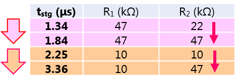
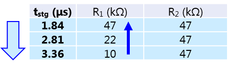
BRTs are mainly used as switches and remain in the saturation region while they are on. Therefore, the storage time (tstg), i.e., the time required to remove minority carriers from the base, accounts for the dominant portion of the switching time.
There are two considerations for reducing tstg:
a) Removing excessive carriers quickly
Excessive carriers accumulated in the base are removed mainly through R2 although the carrier removal path slightly differs, depending on the configuration of the preceding circuit. (If the output of the preceding circuit has low impedance at Low level, excessive carriers are also removed through R1). Therefore, BRTs with a low R2 value are suitable for increasing the switching speed.
b) Minimize the accumulation of excessive carriers.
This means that the depth of saturation of the BRT is reduced while it is on. To minimize the accumulation of excessive carriers, it is necessary to reduce the current applied to the base of the internal transistor (Ib). This can be achieved by 1) reducing the input current to the BRT (IB) and 2) reducing the base current of the internal transistor (i.e., increasing the current flowing to R2). Therefore, BRTs with a large R1 value and a large resistor ratio (R1/R2) are suitable. Note, however, that minimizing the accumulation of excessive carriers might reduce the depth of saturation, causing VCE(sat) to increase.