
- General Top
- SEMICONDUCTOR
- STORAGE
- COMPANY
-
My ToshibaSemicon
- Semiconductor Top
-
ApplicationsAutomotive
Body Electronics
xEV
In-Vehicle Infotainment
Advanced Driver-Assistance Systems (ADAS)
Chassis
IndustrialInfrastructure
BEMS/HEMS
Factory Automation
Commercial Equipment
Consumer/PersonalIoT Equipment
Healthcare
Wearable Device
Mobile
Computer Peripherals
-
ProductsAutomotive Devices
Discrete Semiconductor
Diodes
Transistors
Logic ICs
Analog Devices
- Automotive SmartMCD™ (Integreted SoC Conbining Microcontroller and Driver)
- Automotive Brushless Motor Driver ICs
- Automotive Brushed DC Motor Driver ICs
- Automotive Stepping Motor Driver ICs
- Automotive Driver ICs
- Automotive System Power Supplies ICs
- Automotive audio power amplifier ICs
- Automotive Network Communication
Digital Devices
Wireless Devices
※
 : Products list (parametric search)Power Semiconductors
SiC Power Devices
※
: Products list (parametric search)Isolators/Solid State RelaysPhotocouplers
Digital Isolators
Solid State Relays
Fiber Optic Transmitting Modules
※
: Products list (parametric search)MOSFETsIGBTs/IEGTsBipolar Transistors※
: Products list (parametric search)Diodes※
: Products list (parametric search)MicrocontrollersMotor Driver ICsIntelligent Power ICs※
: Products list (parametric search)Power Management ICsLinear ICs※
: Products list (parametric search)General Purpose Logic ICsLinear Image SensorsOther Product ICsOther Product ICs
※
: Products list (parametric search) -
Design & Development
Design & Development
Innovation Centre
At the Toshiba Innovation Centre we constantly strive to inspire you with our technologies and solutions. Discover how to place us at the heart of your innovations.
-
Knowledge
Knowledge
Highlighted Topics
Further Materials
Other
- Where To Buy


- Part Number & Keyword Search
- Cross Reference Search
- Parametric Search
- Stock Check & Purchase
This webpage doesn't work with Internet Explorer. Please use the latest version of Google Chrome, Microsoft Edge, Mozilla Firefox or Safari.
require 3 characters or more. Search for multiple part numbers fromhere.
The information presented in this cross reference is based on TOSHIBA's selection criteria and should be treated as a suggestion only. Please carefully review the latest versions of all relevant information on the TOSHIBA products, including without limitation data sheets and validate all operating parameters of the TOSHIBA products to ensure that the suggested TOSHIBA products are truly compatible with your design and application.Please note that this cross reference is based on TOSHIBA's estimate of compatibility with other manufacturers' products, based on other manufacturers' published data, at the time the data was collected.TOSHIBA is not responsible for any incorrect or incomplete information. Information is subject to change at any time without notice.
require 3 characters or more.
RF SPDT (Single-Pole Double-Throw that realizes high-power input in a small package.)
Toshiba Electronic Devices & Storage Corporation just released RF SPDT switching TCWA1225G with a compact package. TCWA1225G uses Toshiba original CMOS Process for RF transmission path switching circuits used in telecommunications base stations and radio communications equipment. Starts shipping.
In recent years, telecommunications base stations have introduced Massive MIMO[Note 1] and other that use several transmitting and receiving antennas to realize ultra-high-speed and ultra-large-capacity radio communications services. This is represented by 5G. Individual antennas are also increasingly composed of super-multi-element antennas and complex signal transmission paths. When switching between such complex transmission paths, RF switching is generally used. However, this RF must have low insertion-loss, high input-power, etc. It is also required to be small enough so that the number of RF switches will not increase, and the size of antennas and devices will not increase.
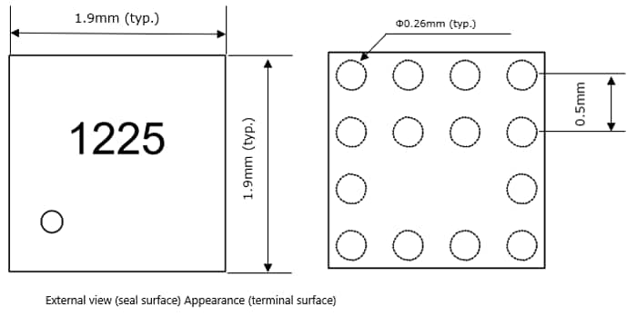
The new TCWA1225G offers a high-power, Peak Power Handling Rating 46dBm[Note 2] in a small package of 1.9mm×1.9mm (typ.) , thus contributing to the miniaturization of equipment. In addition, since the insertion loss 0.6dB[Note 3] and the power consumption current are as low as 50μA[Note 4], it contributes to reducing the loss and power consumption of equipment.
Switching can be easily controlled via the built-in GPIO control interface.
[Note 1] Multiple Input Multiple Output
[Note 2] 8dB PAR (Peak-to-Average Ratio)
[Note 3] 5GHz, typical
[Note 4] VDD=3.6V, typical
Main features of the new product
- Small packages
- High-power input
- Low insertion loss
Features Explanation
1. Small packages
2.0mm x 2.0mm (typ.) is the smallest Competitor's alternative with equivalent performance for high-power input RF SPDT switches, but 1.9mm × 1.9mm (typ.) is a small WCSP[Note 5] with approximately 10% less mounting area. The highly versatile 0.5mm also eliminates the need for sophisticated mounting techniques and reduces the possibility of short-circuit between terminals during board mounting. In addition, RF terminal, power supply, and control terminal are arranged on the periphery of the package to prevent complicated pattern-design of the board.
[Note 5] Wafer level Chip Scale Package
2. High-power input
In order to achieve both miniaturization and high-power inputting, we adopted Toshiba original CMOS process and further optimized the switching circuitry. This has resulted in a small size and 46dBm high-power input 1.9mm × 1.9mm (typ.)[Note 6] compared to 2.0mm x 2.0mm (typ.) packaged and 42dBm peak input power.
3. Low insertion loss
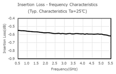
In the transmission path switching circuitry of RF signals, RF signal must be made extremely small to prevent a decrease in transmit power and a deterioration in receiver sensitivity. TCWA1225G is to achieve 0.6dB (typ.) @5GHz and an insertion-loss that is approximately 0.05dB smaller than Competitor's alternative with equivalent performance.[Note 6] This is achieved by using Toshiba original CMOS Process.
[Note 6] Comparison with similar products. Our survey as of June 2024.
Applied equipment
- Communication base station
- Wireless communication equipment
- Other communications equipment
Main specifications of the product
(Ta=25°C)
Product Number |
||
|---|---|---|
Data Sheet |
||
Absolute maximum ratings |
Supply voltage Range VDD(V) |
-0.3 to 3.9 |
Logic Input (LS, CTRL Pad) Vl(V) |
-0.3 to 3.9 |
|
Peak Power Handling (8dB PAR) Ppk(dBm) |
46 |
|
| Operating ranges | Supply voltage VDD(V) |
3.0 to 3.6 |
| Operation Temperature Topr(°C) |
-40 to 95 |
|
Electrical characteristics (Typ.)
|
Insertion loss IL(dB)@5GHz |
0.6 |
Isolation ISO(dB)@5GHz |
46 |
|
VSWR (-) |
1.2 |
|
Input 1dB compression IP1dB(dBm)@2.6GHz |
47 |
|
Input IP3 IIP3(dBm)@2.6GHz |
74 |
|
Input IP2 IIP2(dBm)@2.6GHz |
128 |
|
Power Consumption Current IDC(μA)@VDD=3.6V |
50 |
|
Package |
Toshiba name |
|
Sizing(mm) Typ. |
1.9 × 1.9 |
|
Inventory retrieval & Web small buy |
|
|

Relevant information
Product detail
Package
*Company names, product names, and service names may be trademarks of their respective companies.
*Information contained in this document (product price/specifications, service details, inquiries, etc.) is as of the date of presentation. This manual is subject to change without prior notice.