
-
My ToshibaSemicon
- 반도체 탑
-
애플리케이션Automotive
Body Electronics
xEV
In-Vehicle Infotainment
Advanced Driver-Assistance Systems (ADAS)
Chassis
IndustrialInfrastructure
BEMS/HEMS
Factory Automation
Commercial Equipment
Consumer/PersonalIoT Equipment
Healthcare
Wearable Device
Mobile
Computer Peripherals
-
제품자동차 디바이스
Discrete Semiconductor
다이오드
트랜지스터
로직 IC
Analog Devices
Digital Devices
Wireless Devices
※
 : Products list (parametric search)파워반도체
※
: Products list (parametric search)Isolators/Solid State RelaysPhotocouplers
Digital Isolators
Solid State Relays
Fiber Optic Transmitting Modules
※
: Products list (parametric search)MOSFETsIGBTs/IEGTs바이폴라 트랜지스터※
: Products list (parametric search)다이오드※
: Products list (parametric search)마이크로컨트롤러모터 드라이버 ICIntelligent Power ICs※
: Products list (parametric search)전원관리IC리니어 IC※
: Products list (parametric search)범용로직IC리니어 이미지 센서기타 제품용 IC기타 제품용 IC
※
: Products list (parametric search) -
개발/설계 지원
-
기술 자료
- 구매처


- 부품 번호 & 키워드 검색
- 상호 참조 검색
- 파라미터 검색
- 재고 확인 및 구매
This webpage doesn't work with Internet Explorer. Please use the latest version of Google Chrome, Microsoft Edge, Mozilla Firefox or Safari.
3글자 이상 입력하세요. Search for multiple part numbers fromhere.
The information presented in this cross reference is based on TOSHIBA's selection criteria and should be treated as a suggestion only. Please carefully review the latest versions of all relevant information on the TOSHIBA products, including without limitation data sheets and validate all operating parameters of the TOSHIBA products to ensure that the suggested TOSHIBA products are truly compatible with your design and application.Please note that this cross reference is based on TOSHIBA's estimate of compatibility with other manufacturers' products, based on other manufacturers' published data, at the time the data was collected.TOSHIBA is not responsible for any incorrect or incomplete information. Information is subject to change at any time without notice.
3글자 이상 입력하세요.
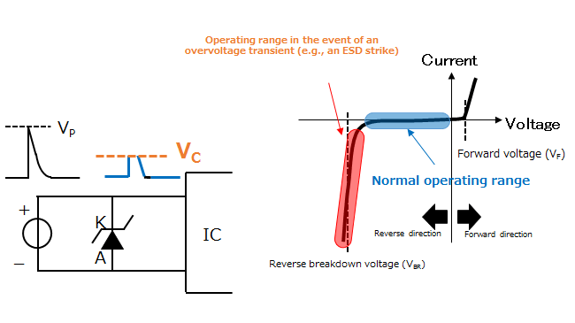
1-1 Reverse breakdown voltage
The reverse breakdown voltage is determined by Zener breakdown or avalanche breakdown.
Zener breakdown
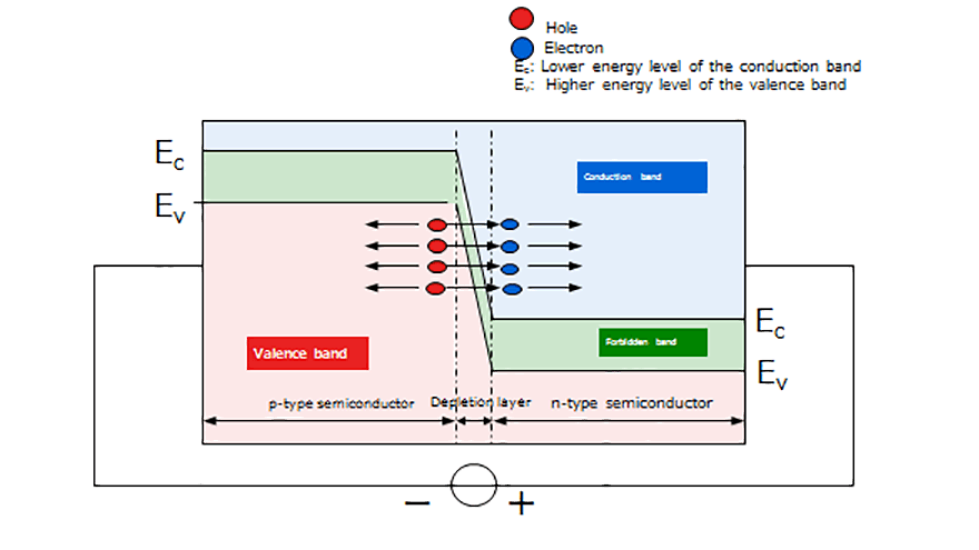
When a pn junction is reverse-biased, a depletion layer extends across the pn junction. An electric field causes a gap between the valence band of the p-type region and the conduction band of the n-type region to decrease inside the depletion layer. As a result, electrons tunnel from the valence band of the p-type region to the conduction band of the n-type region because of quantum tunneling. Zener breakdown is a phenomenon in which the tunneling of electrons across the depletion region causes a sudden increase in reverse current. Figure 1.3 illustrates Zener breakdown.
Avalanche breakdown
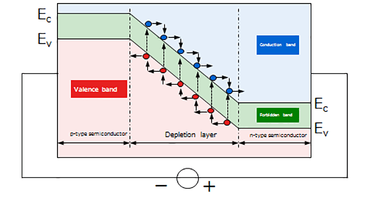
When a pn junction is reverse-biased, a small quantity of electrons passes through the pn junction. These electrons are accelerated in the depletion layer by an electric field, acquiring large kinetic energy. The accelerated electrons collide with the atoms in a crystal lattice, ionizing them and creating electron holes. The electrons of these atoms are excited to the conduction band and knocked out, becoming free electrons. The free electrons are also accelerated and collide with other atoms, creating more electron-hole pairs and leading to further knocking-out processes. This phenomenon is called avalanche breakdown.
Comparison of avalanche breakdown and Zener breakdown
Since diodes with high breakdown voltage are lightly doped, they form a wide depletion layer (forbidden band). Conversely, since diodes with low breakdown voltage are heavily doped, they form a thin depletion layer (forbidden band). When a diode has a wide depletion layer, electron tunneling (Zener breakdown) is less likely to occur, causing avalanche breakdown to become more predominant. In the case of a heavily doped diode with a thin depletion layer, Zener breakdown is more like to occur. As temperature increases, the width of the forbidden band (Eg) decreases, contributing to the Zener effect. In addition, as temperature increases, the lattice vibration of a semiconductor increases, causing its carrier mobility to decrease. As a result, avalanche breakdown becomes less likely to occur. Zener breakdown voltage decreases with temperature whereas avalanche breakdown voltage increases with temperature. Generally, Zener breakdown is predominant below roughly 6 V whereas avalanche breakdown is predominant above roughly 6 V. It should be noted that even diodes of the same product series exhibit different temperature characteristics.
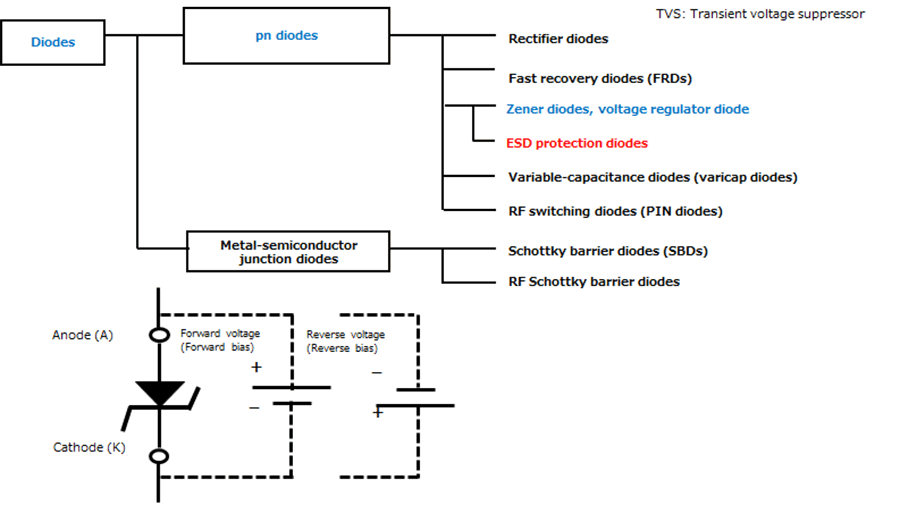
1 What is a TVS diode (ESD protection diode)?
- 2 Basic operations of TVS diodes (ESD protection diodes)
- 3 Key electrical characteristics of TVS diodes (ESD protection diodes)
- 4 Selection guidelines for TVS diodes (ESD protection diodes)
- 5 Layout considerations for TVS diodes (ESD protection diodes)
- 6 Absolute maximum ratings of TVS diodes (ESD protection diodes)
- 7 Electrical characteristics of TVS diodes (ESD protection diodes)
Related information
- Product Web Page
TVS Diodes (ESD protection diodes) - Applidcation Notes
Diode - FAQ
TVS diodes (ESD protection diodes) - Parametric searches for all Toshiba TVS diode (ESD protection diodes) produ cts are available here:
Parametric search - Stock Check & Purchase Toshiba TVS diode (ESD protection diodes) here
Stock Check & Purchase