-
My ToshibaSemicon
- 반도체 탑
-
애플리케이션Automotive
Body Electronics
xEV
In-Vehicle Infotainment
Advanced Driver-Assistance Systems (ADAS)
Chassis
IndustrialInfrastructure
BEMS/HEMS
Factory Automation
Commercial Equipment
Consumer/PersonalIoT Equipment
Healthcare
Wearable Device
Mobile
Computer Peripherals
-
제품자동차 디바이스
Discrete Semiconductor
다이오드
트랜지스터
로직 IC
Analog Devices
Digital Devices
Wireless Devices
※
 : Products list (parametric search)파워반도체
※
: Products list (parametric search)Isolators/Solid State RelaysPhotocouplers
Digital Isolators
Solid State Relays
Fiber Optic Transmitting Modules
※
: Products list (parametric search)MOSFETsIGBTs/IEGTs바이폴라 트랜지스터※
: Products list (parametric search)다이오드※
: Products list (parametric search)마이크로컨트롤러모터 드라이버 ICIntelligent Power ICs※
: Products list (parametric search)전원관리IC리니어 IC※
: Products list (parametric search)범용로직IC리니어 이미지 센서기타 제품용 IC기타 제품용 IC
※
: Products list (parametric search) -
개발/설계 지원
-
기술 자료
- 구매처


- 부품 번호 & 키워드 검색
- 상호 참조 검색
- 파라미터 검색
- 재고 확인 및 구매
This webpage doesn't work with Internet Explorer. Please use the latest version of Google Chrome, Microsoft Edge, Mozilla Firefox or Safari.
3글자 이상 입력하세요. Search for multiple part numbers fromhere.
The information presented in this cross reference is based on TOSHIBA's selection criteria and should be treated as a suggestion only. Please carefully review the latest versions of all relevant information on the TOSHIBA products, including without limitation data sheets and validate all operating parameters of the TOSHIBA products to ensure that the suggested TOSHIBA products are truly compatible with your design and application.Please note that this cross reference is based on TOSHIBA's estimate of compatibility with other manufacturers' products, based on other manufacturers' published data, at the time the data was collected.TOSHIBA is not responsible for any incorrect or incomplete information. Information is subject to change at any time without notice.
3글자 이상 입력하세요.
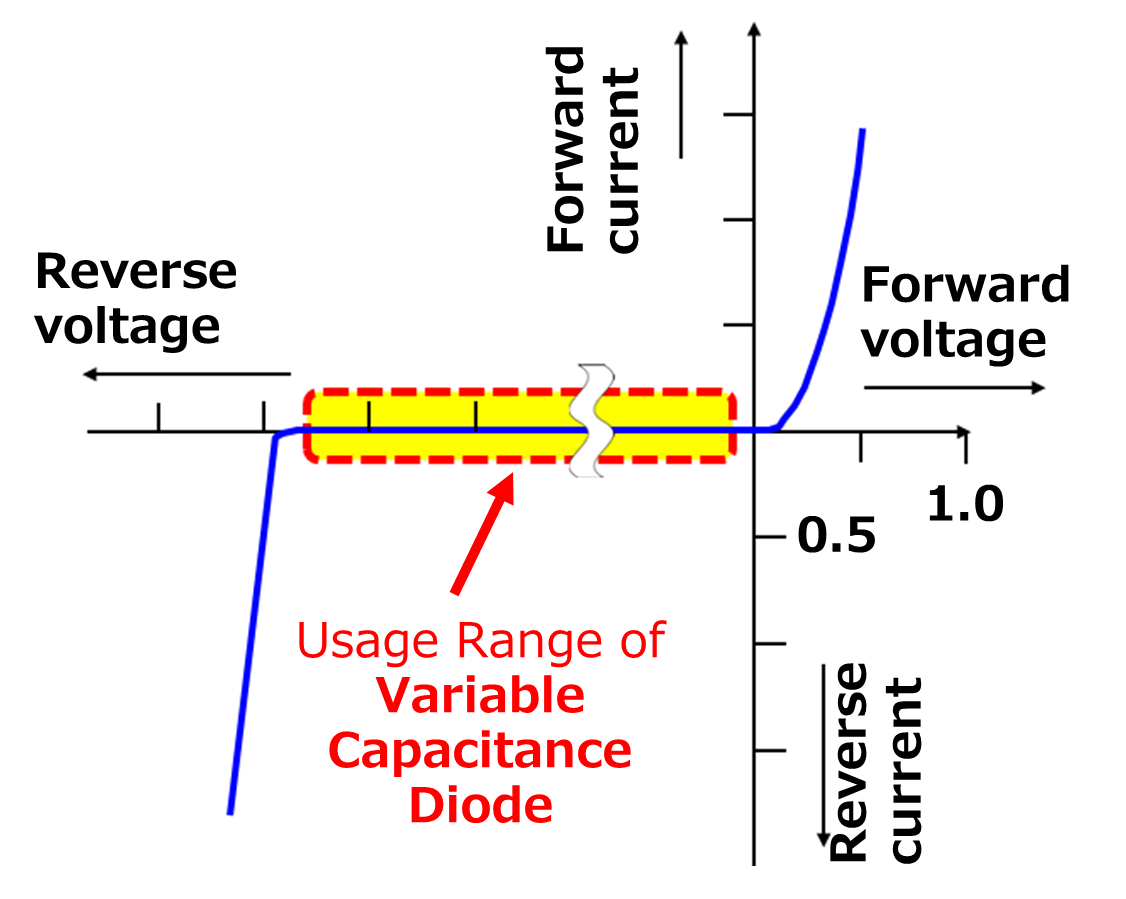
What is a variable-capacitance (varicap) diode?
A varicap diode is a product that utilizes depletion layer capacitance characteristics generated when reverse voltage is applied to a PN junction. The depletion layer works as a gap between electrodes. Capacity varies as the depletion layer changes according to the applied voltage.
A variable-capacitance diode is a type of pn junction diode. Unlike typical pn junction diodes, variable-capacitance diodes are used in regions where the pn junction is reverse-biased but does not enter breakdown.
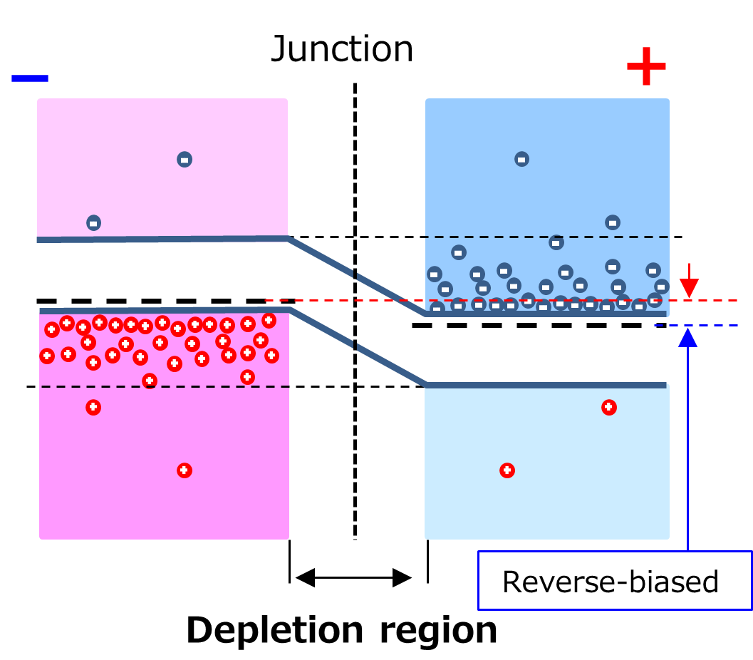
a pn junction diode, a depletion region is formed around the pn junction as shown in the following band diagram (Fig. 2). In a pn junction diode, a depletion region is formed around the pn junction as shown in the following band diagram (Fig. 2). The depletion region has high electrical resistance like an insulator due to the depletion of mobile carriers. In this state, the depletion region behaves like a capacitor. The depletion region widens in proportion to reverse voltage.
Variable-capacitance diodes are designed to exploit this voltage-dependent capacitance of the depletion region.
Capacitance is expressed as follows:
C=K x ( VR + Φ )-n
K: Device-specific constant determined by dopant concentration, junction area, etc.
Φ: Diffusion potential
There are several types of pn junctions including linearly graded, abrupt, and hyper-abrupt junctions. Variable n in the above equation depends on the type of junction. n is 1/3, 1/2, or 1 or greater for linearly graded, abrupt, and hyper-abrupt junctions, respectively. The rate of change in capacitance increases with the value of n. Typical pn junction diodes such as switching diodes have an oblique junction whereas variable-capacitance diodes have an abrupt or hyper-abrupt junction.

Related Links
For products, please refer to the following links.