-
My ToshibaSemicon
- 홈페이지 보기
-
반도체 보기
-
애플리케이션
Body Electronics
xEV
In-Vehicle Infotainment
Advanced Driver-Assistance Systems (ADAS)
Chassis
Infrastructure
BEMS/HEMS
Factory Automation
Commercial Equipment
IoT Equipment
Healthcare
Wearable Device
Mobile
Computer Peripherals
-
제품
*
 : Products list (parametric search)
Photocouplers
Digital Isolators
Solid State Relays
Fiber Optic Transmitting Modules
*
: Products list (parametric search)*
: Products list (parametric search)*
: Products list (parametric search)*
: Products list (parametric search)Discrete Semiconductor
다이오드
트랜지스터
로직 IC
Analog Devices
Digital Devices
Wireless Devices
*
: Products list (parametric search)*
: Products list (parametric search)*
: Products list (parametric search)*
: Products list (parametric search) -
개발/설계 지원
-
기술 자료
- 구매처 보기
-
- 스토리지 보기
- 회사 개요 보기


- 부품 번호 검색
- 상호 참조 검색
- 키워드 검색
- 파라미터 검색
- 재고 확인 및 구매
This webpage doesn't work with Internet Explorer. Please use the latest version of Google Chrome, Microsoft Edge, Mozilla Firefox or Safari.
3글자 이상 입력하세요.
The information presented in this cross reference is based on TOSHIBA's selection criteria and should be treated as a suggestion only. Please carefully review the latest versions of all relevant information on the TOSHIBA products, including without limitation data sheets and validate all operating parameters of the TOSHIBA products to ensure that the suggested TOSHIBA products are truly compatible with your design and application.Please note that this cross reference is based on TOSHIBA's estimate of compatibility with other manufacturers' products, based on other manufacturers' published data, at the time the data was collected.TOSHIBA is not responsible for any incorrect or incomplete information. Information is subject to change at any time without notice.
3글자 이상 입력하세요.
At what voltages does the bias resistor built-in transistor (BRT) turn on and off?
The turn-on and turn-off thresholds are defined as “input voltage (ON)” (VIN(ON)) and “input voltage (OFF)” (VIN(OFF)) respectively in the datasheet.
- Input voltage (ON), VIN(ON): Voltage required to obtain the collector current equal to or higher than the prescribed value (e.g., IC ≥ 5 mA) at Ta = 25°C
- Input voltage (OFF), VIN(OFF): Voltage required to keep the collector current below the prescribed value (e.g., IC ≤ 0.1 mA) at Ta = 25°C
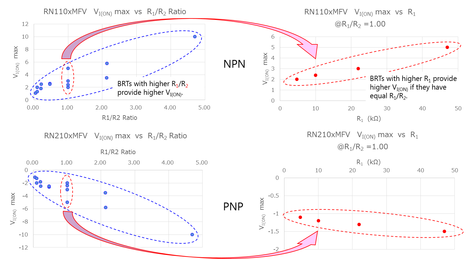
Let’s consider the case in which an NPN BRT turns on.
When the NPN BRT is off, its internal transistor Q is inactive. Therefore, the input voltage (VI) applied to the B terminal is divided by R1 and R2 and then applied to the base (b) of Q. As VI increases, the base-emitter (b-e) voltage (Vbe) exceeds the threshold (typically 0.7 V), turning on Q. The input voltage (ON) is defined as the voltage required to provide a collector current of 5 mA or more, but the concept is the same.
Therefore, BRTs with a lower resistor ratio (R1/R2) reach the threshold voltage at a lower input voltage (VIN(ON)). However, BRTs with a larger R1 value provide lower IB if their resistor ratio is equal.
For example, let the input voltage required to provide a collector current of 5 mA be VI1. Then, the base current ib and the b-e voltage Vbe of the built-in transistor are constant at ib1 and Vbe1 respectively regardless of the built-in resistance. Vin can be expressed as follows using these variables:
Vin1 = R1 * Ib1 + ( 1 + R1 / R2 ) * Vbe
At a given resistance ratio, only the first term “R1 * Ib” on the right side changes. Therefore, it can be considered that Vin1 increases as R1 increases. (See Figure 3.)
Likewise, BRTs with a lower resistor ratio exhibit lower input voltage (OFF). However, the relationship between the resistor ratio and the input voltage (OFF) is less marked than the relationship between the resistor ratio and the input voltage (ON) because the test condition for the input voltage (OFF) is as low as 0.1 mA and therefore tends to be affected by device variations.
The above discussion also applies to PNP BRTs although their numeric sign is the opposite to that of NPN BRTs.
The IC – VI(ON) curves of Figure 2 show that the collector current changes suddenly at a given input voltage. The collector current also decreases as temperature increases. Make sure you allow for sufficient design margins.

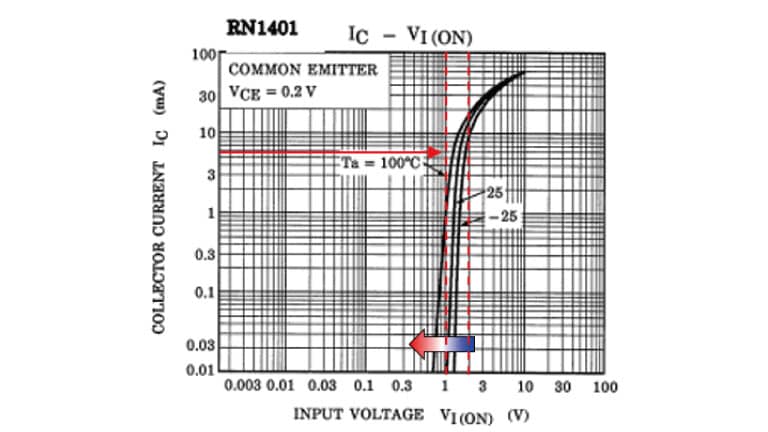
| Characteristic | Symbol | Test Condition | Min | Typ. | Max | Unit | |
|---|---|---|---|---|---|---|---|
Input voltage (ON) |
RN1401 | VI (ON) | VCE = 0.2 V, IC = 5 mA |
1.1 | — | 2.0 | V |