- General Top
- SEMICONDUCTOR
- STORAGE
- COMPANY
-
My ToshibaSemicon
- Semiconductor Top
-
ApplicationsAutomotive
Body Electronics
xEV
In-Vehicle Infotainment
Advanced Driver-Assistance Systems (ADAS)
Chassis
IndustrialInfrastructure
BEMS/HEMS
Factory Automation
Commercial Equipment
Consumer/PersonalIoT Equipment
Healthcare
Wearable Device
Mobile
Computer Peripherals
-
ProductsAutomotive Devices
Discrete Semiconductor
Diodes
Transistors
Logic ICs
Analog Devices
- Automotive SmartMCD™ (Integreted SoC Conbining Microcontroller and Driver)
- Automotive Brushless Motor Driver ICs
- Automotive Brushed DC Motor Driver ICs
- Automotive Stepping Motor Driver ICs
- Automotive Driver ICs
- Automotive System Power Supplies ICs
- Automotive audio power amplifier ICs
- Automotive Network Communication
Digital Devices
Wireless Devices
※
 : Products list (parametric search)Power Semiconductors
SiC Power Devices
※
: Products list (parametric search)Isolators/Solid State RelaysPhotocouplers
Digital Isolators
Solid State Relays
Fiber Optic Transmitting Modules
※
: Products list (parametric search)MOSFETsIGBTs/IEGTsBipolar Transistors※
: Products list (parametric search)Diodes※
: Products list (parametric search)MicrocontrollersMotor Driver ICsIntelligent Power ICs※
: Products list (parametric search)Power Management ICsLinear ICs※
: Products list (parametric search)General Purpose Logic ICsLinear Image SensorsOther Product ICsOther Product ICs
※
: Products list (parametric search) -
Design & Development
Design & Development
Innovation Centre
At the Toshiba Innovation Centre we constantly strive to inspire you with our technologies and solutions. Discover how to place us at the heart of your innovations.
-
Knowledge
Knowledge
Highlighted Topics
Further Materials
Other
- Where To Buy


- Part Number & Keyword Search
- Cross Reference Search
- Parametric Search
- Stock Check & Purchase
This webpage doesn't work with Internet Explorer. Please use the latest version of Google Chrome, Microsoft Edge, Mozilla Firefox or Safari.
require 3 characters or more. Search for multiple part numbers fromhere.
The information presented in this cross reference is based on TOSHIBA's selection criteria and should be treated as a suggestion only. Please carefully review the latest versions of all relevant information on the TOSHIBA products, including without limitation data sheets and validate all operating parameters of the TOSHIBA products to ensure that the suggested TOSHIBA products are truly compatible with your design and application.Please note that this cross reference is based on TOSHIBA's estimate of compatibility with other manufacturers' products, based on other manufacturers' published data, at the time the data was collected.TOSHIBA is not responsible for any incorrect or incomplete information. Information is subject to change at any time without notice.
require 3 characters or more.
Accelerating EV Charging System Development: New PFC Reference Design Proves Invaluable Tool

The number of electric vehicles (EVs) on our roads is set to increase dramatically in the years ahead, with 323 million of them being in use by 2040 (according to a study compiled by analyst firm Wood Mackenzie). Alongside this ramped up EV production, there will need to be major investments in charging infrastructure. Amongst the places where demand will be at its most acute is within emerging economies, but here the level of technical expertise needed to develop charging stations that exhibit high degrees of efficiency within short the time frames mandated will be very limited.
In response to these dynamics, Toshiba has developed a 3-phase 400VAC input power system reference design which is well suited to the demands of EV charging infrastructure implementations. The RD044-DGUIDE-01 leverages the latest innovations in widebandgap discretes. Requiring only minimal engineering resources, it will help to enable next generation charging station designs to be undertaken in a shorter timeframe.
Featuring power factor correction (PFC) functionality, the RD044-DGUIDE-01 reference design has a power factor greater than 0.99. Using this hardware, initial prototypes can be quickly constructed and their operational parameters examined prior to moving into the production stage. It is able to deliver a 4kW, 750VDC output - with support for switching frequencies of up to 50kHz and conversion efficiencies reaching 97%. As a totem pole configuration is employed in this reference design, each phase is switched directly. This dispenses with the need for a diode bridge rectifier - which would present large losses given the high power figures involved, thereby impacting on the conversion efficiencies that could be derived.
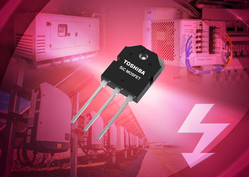
Pivotal to this reference design’s operation is the TW070J120B N-channel silicon carbide (SiC) MOSFET that has been incorporated. The three-phase 400VAC input means that the totem pole configuration needs an elevated withstand voltage for its switching elements (with the capacity to cope with voltages of at least 1000V). Under such circumstances, IGBTs would normally be sourced. However, IGBTs possess slower switching speeds than MOSFETs and have greater switching losses associated with them. By using MOSFETs that are based on SiC, it is possible to benefit from a combination of accelerated switching speeds and elevated withstand voltages. Featuring a built-in SiC Schottky barrier diode, the TW070J120B has a 1200V withstand voltage and a threshold (Vth) of 4.2V to 5.8V. Its on-state resistance is just 70mΩ, which helps to mitigate power losses.
Via the TLP5214A gate driver IC that the reference design also includes, it is possible to alter the switching speed of the MOSFET. This means that the engineer can make adjustments to the switching drive conditions while monitoring the electro-magnetic interference (EMI) effects, so that an optimal balance can be decided upon.
Toshiba has published a white paper describing the RD044-DGUIDE-01 reference design in detail, and showing how it can facilitate the development of advanced EV charging systems. To download it click here: