- General Top
- SEMICONDUCTOR
- STORAGE
- COMPANY
-
My ToshibaSemicon
- Semiconductor Top
-
ApplicationsAutomotive
Body Electronics
xEV
In-Vehicle Infotainment
Advanced Driver-Assistance Systems (ADAS)
Chassis
IndustrialInfrastructure
BEMS/HEMS
Factory Automation
Commercial Equipment
Consumer/PersonalIoT Equipment
Healthcare
Wearable Device
Mobile
Computer Peripherals
-
ProductsAutomotive Devices
Discrete Semiconductor
Diodes
Transistors
Logic ICs
Analog Devices
- Automotive SmartMCD™ (Integreted SoC Conbining Microcontroller and Driver)
- Automotive Brushless Motor Driver ICs
- Automotive Brushed DC Motor Driver ICs
- Automotive Stepping Motor Driver ICs
- Automotive Driver ICs
- Automotive System Power Supplies ICs
- Automotive audio power amplifier ICs
- Automotive Network Communication
Digital Devices
Wireless Devices
※
 : Products list (parametric search)Power Semiconductors
SiC Power Devices
※
: Products list (parametric search)Isolators/Solid State RelaysPhotocouplers
Digital Isolators
Solid State Relays
Fiber Optic Transmitting Modules
※
: Products list (parametric search)MOSFETsIGBTs/IEGTsBipolar Transistors※
: Products list (parametric search)Diodes※
: Products list (parametric search)MicrocontrollersMotor Driver ICsIntelligent Power ICs※
: Products list (parametric search)Power Management ICsLinear ICs※
: Products list (parametric search)General Purpose Logic ICsLinear Image SensorsOther Product ICsOther Product ICs
※
: Products list (parametric search) -
Design & Development
Design & Development
Innovation Centre
At the Toshiba Innovation Centre we constantly strive to inspire you with our technologies and solutions. Discover how to place us at the heart of your innovations.
-
Knowledge
Knowledge
Highlighted Topics
Further Materials
Other
- Where To Buy


- Part Number & Keyword Search
- Cross Reference Search
- Parametric Search
- Stock Check & Purchase
This webpage doesn't work with Internet Explorer. Please use the latest version of Google Chrome, Microsoft Edge, Mozilla Firefox or Safari.
require 3 characters or more. Search for multiple part numbers fromhere.
The information presented in this cross reference is based on TOSHIBA's selection criteria and should be treated as a suggestion only. Please carefully review the latest versions of all relevant information on the TOSHIBA products, including without limitation data sheets and validate all operating parameters of the TOSHIBA products to ensure that the suggested TOSHIBA products are truly compatible with your design and application.Please note that this cross reference is based on TOSHIBA's estimate of compatibility with other manufacturers' products, based on other manufacturers' published data, at the time the data was collected.TOSHIBA is not responsible for any incorrect or incomplete information. Information is subject to change at any time without notice.
require 3 characters or more.
Why Designers are Looking to SiC for Bidirectional DC-DC Converters
With pressure to reduce reliance on fossil fuels and other polluting energy sources, electrical energy becomes the preferred choice. The most obvious change is the automotive industry’s move to partial or full electrical power. With electric vehicle (EV) chargers delivering between 3.6 kW and 22 kW of energy during charging and up to 150 kW in fast DC chargers, every percentage point of efficiency improvement implies several hundred Watts of energy that need not be dissipated as heat. This enables designers to build smaller, lighter designs or more powerful solutions into existing form factors. Adding to the challenge, automotive OEMs are planning to support bidirectional power flow, enabling EVs to jump-start other EVs, power conventional appliances while camping, or even help to balance the electrical grid to avoid brown-outs.
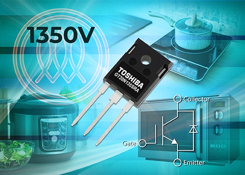
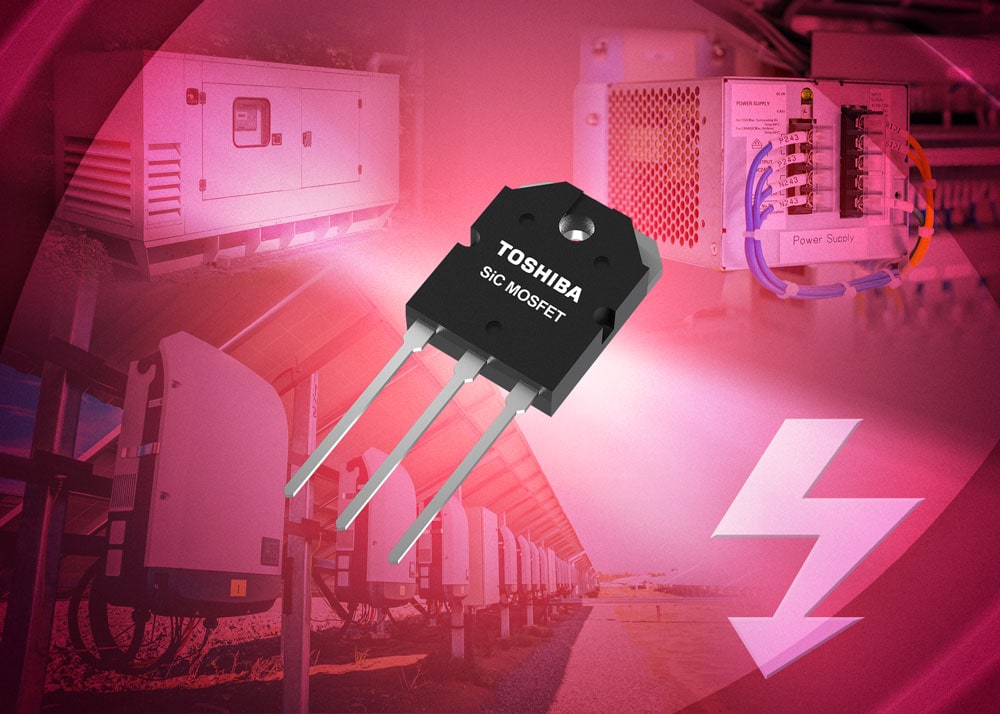
Traditionally, IGBTs have been the chosen power device for the high-voltage stages of DC-DC converters. Robust and well understood, they have steadily improved in their switching speed allowing progress to be made in power converter designs. However, thanks to wide-bandgap (WBG) technology developments, silicon carbide (SiC) is increasingly the preferred choice in such applications. With significantly faster turn-on and turn-off speeds, the switching losses in SiC devices, such as the 1200 V Toshiba TW070J120B N-channel MOSFET with built-in SiC Schottky barrier diode, contribute to a 66% reduction in power losses compared with a comparable IGBT in the same application.
Topologies such as Dual Active Bridge (DAB) are often found in existing EV chargers and referenced in research in this area. Its high-frequency transformer provides the required galvanic isolation. Due to the lower voltages on the DC load side charging the battery, next generation silicon MOSFETs offer an optimal price-performance point. Devices such as the TK49N65W5, a DTMOS superjunction N-channel device offering superior RDS(ON) and fast reverse recovery time (trr), coupled with the TLP5214A gate driver, make for an ideal choice to complement the SiC MOSFETs for a highly efficient design.
These devices’ full capability is realized in Toshiba’s latest reference design, a 50 kHz switching, isolated bidirectional DC-DC power supply. Designed to support power converter designers working on high-power designs, the design handles up to 5 kW from a 750 V DC link. This forms an excellent starting point for EV charger developers. At a 100% step-up/-down load, the design has shown to operate with efficiencies of 97%.
The full details of this reference design, along with the advantages SiC MOSFETs offer over traditional IGBT-based designs, are shared in our latest white paper available here: