What is the tolerant function of the general-purpose logic ICs?
Tolerant means "with tolerance", and is a function that does not malfunction or damage even if a voltage higher than the IC's power supply voltage* is applied to the input or output terminals. General-purpose logic IC has two types of tolerant functions: input-tolerant and output-tolerant. If the supply voltage of general purpose logic IC may be exceeded, you must select a device that has this function. This is one of the most important characteristics. (*: Voltage exceeding the input/output voltage of absolute maximum ratings cannot be applied)
Electronic devices contain multiple ICs that sometimes operate in different voltage domains (e.g., 3.3-V and 5-V domains). In this case, you need general purpose logic ICs with input- and output-tolerant functions as well as a level-shifting function (described later).
Many mobile devices incorporate a partial power-down function, which shuts down unused logic blocks to save power and prolong the battery operating time. To realize partial power-down, output power-down protection is necessary. (Refer to Note described later)
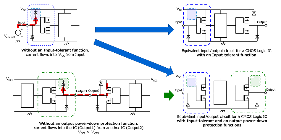
- Input tolerant: While VCC is active (within the operating voltage range) or VCC = 0, this function prevents current from flowing into an IC when the input voltage is higher than the supply voltage (VCC). However, it is not permitted to apply a voltage higher than the maximum operating voltage to the input pin.
The tolerant function of an output pin is more complicated. The output circuitry of CMOS logic ICs has a totem-pole structure consisting of a pair of P-channel and N-channel MOSFETs as shown in Fig. 1. Therefore, most CMOS logic ICs do not permit external voltage application to the output pin while they are active. If voltage is applied to the output, it is short-circuited to the power supply or GND, possibly leading to the destruction of the IC.

- Output tolerant: Output tolerant is a function that avoids current flow from the output pins to the IC (leak-level current flows) when the IC is in disable mode and the output is Hi-Z, even if a voltage exceeding the supply voltage is applied to the output pins. However, a voltage exceeding the power supply voltage cannot be applied in the enable state (High or Low). If voltage is applied to the output, the output is short-circuited to the power supply or GND, possibly leading to the destruction of the IC.
In the case of open-drain ICs with output tolerant functions as well, current does not flow into an IC from an output pin even if a voltage higher than the supply voltage is applied to the output.
In this type, by inserting a resistor between the external power supply and the output, a voltage exceeding the power supply voltage can be applied. However, even in the case of CMOS logic ICs with an output-tolerant function, it is not permitted to apply a voltage higher than the maximum operating voltage to the output.
In addition, there is output power-down protection. - Power-down protection (Note):
This function prevents current from flowing into an IC via an output pin when a voltage in the operating voltage range is applied to the output while the power supply is off (VCC = 0 V). Power-down protection works regardless of whether the IC has Disabled mode
Note: In some cases, tolerant and power down protection are used interchangeably. Input tolerant is sometimes called input power down protection, and output power down protection is sometimes called output tolerant.
As shown in Fig. 2, the equivalent circuits for typical general purpose logic ICs that contain diodes on both the input and output sides. The diodes on the input side are inserted for the purpose of ESD protection. Those on the output side are unintentional parasitic diodes. The diode between the input and the power supply and the one between the output and the power supply might turn on if a voltage higher than VCC is applied or voltage is applied when the IC is off. In this case, the IC might be destroyed by the resulting large current.
When a voltage higher than the power supply voltage VCC is applied to the input pin, a large current flows through the diode in the IC (upper diagram in Fig. 3).
By replacing with a series that has an input tolerant function (series with a mark in the input tolerant column in Table-1), damage to the device can be avoided.
In addition, the output side is not directly connected to the power line, but it may be connected to other bus outputs in a bus system.
In the lower diagram of Fig. 3, when VCC1 is turned off and VCC2 is turned on, current flows from Output2 to Output1.
To avoid this, it is necessary to replace the product with the output tolerant function. Output tolerant functions (voltage can be applied from output-pin within an acceptable range) are allowed only for series with the output power-down protection functions shown in Table-1. In addition, it is limited to the function with output disable (function to make the output high-impedance regardless of the input). This means that products with 3-state outputs (e.g., 74LCX244, 74LCX373) can be used.

Type |
Series Name |
CMOS Logic ICs Series No. |
One-Gate Logic ( L-MOS ) Equivalent |
Operating Voltage Range VCC (V) |
Propagation |
Output Current *2 IOUT (mA) |
Input-Tolerant |
Output Power-down Protection |
|---|---|---|---|---|---|---|---|---|
For 5 V Systems |
Standard |
3 to 18 |
200 |
±0.51 |
△*3 |
- |
||
High Speed |
2 to 6 |
23 |
±4.0 or ±6.0 |
△*3 |
- |
|||
4.5 to 5.5 |
31 |
- | ||||||
Advanced |
2 to 5.5 |
8.5 |
±24 |
- |
- |
|||
4.5 to 5.5 |
9.0 |
|||||||
Very High Speed |
2 to 5.5 |
8.5 |
±8.0 |
● |
- |
|||
10 |
||||||||
4.5 to 5.5 |
9.5 |
● |
●*4 |
|||||
1.8 to 5.5 |
8.5 |
±16 |
● |
● |
||||
For low |
Low Voltage |
1.65 to 3.6 |
6.5 |
±24 |
● |
●*5 |
||
Very Low Voltage |
1.2 to 3.6 |
4.2 |
±24 |
● |
● |
*1: Maximum propagation delay time of typical ICs (TC4001, TC74HC244, TC74HCT244, TC74AC244, TC74ACT244, 74VHC244, 74VHC9541 (An-Yn), VHCT244, VHCV244, 74LCX244, and TC74VCX244) at -40 to 85 °C, except for the TC4001 for which the maximum propagation delay time at 25 °C is shown.
*2: Those output current values are from DC Characteristics table of the datasheet. In addition, they are specified in absolute maximum ratings.
*3: TC4049BF/BP, TC4050BF/BP, TC74HC4049BP/BF/BFT, 74HC4049D, TC74HC4050BP/BF/BFT and 74HC4050D have the input-tolerant function that allows level shifting from a higher voltage to a lower voltage.
*4: The TC7SET series and TC7SZU04/TC7WZU04 does not have an output power-down protection function.
*5: The TC7SZ series in the fSV package do not have an output power-down protection function except those with an open-drain output.
Level shifter (level translation) using an input tolerant function
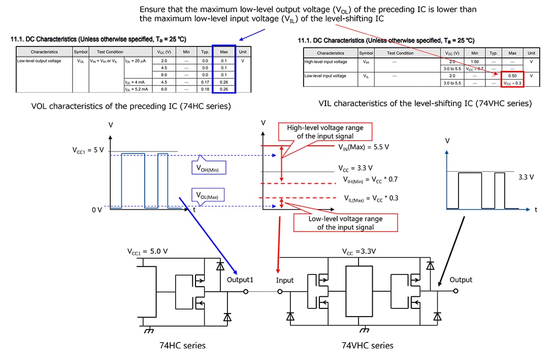
The input-tolerant function can be used to step down the High-level voltage. For example, let’s consider how to step down an output voltage of a logic IC of the HC series from 5 V to 3.3 V using an IC of the VHC series.
For down translation, care should be exercised as to the following characteristics. (The following values are for the VHS series.)
- Input voltage (shown in the Operating Ranges table) VIN(max): 5.5 V
- Maximum Low-level voltage of the preceding IC and Low-level input voltage of the level-shifting IC (shown in the Electrical Characteristics table),
VIL(max) : VCC x 0.3 V - Use the stepped-down voltage (3.3 V in this example) as the supply voltage for the level-shifting general purpose logic IC.
The maximum input voltage must not exceed the value shown in the Operating Ranges table of the datasheet. In addition, the maximum Low-level input voltage must be lower than value shown in the Electrical Characteristics table (VIL).
As long as you pay attention to the above characteristics, you can easily level-shift a logic signal as Fig.
Note, however, that the threshold voltages of 5 V and 3.3 V ICs are different. Therefore, the duty cycle of the logic signal might change as a result of level-shifting.
If this is a concern, use Toshiba’s dual-supply level shifter that provides level-shifting without affecting a duty cycle.
Related Links
The following documents also contain related information.