
-
My ToshibaSemicon
- 반도체 탑
-
애플리케이션Automotive
Body Electronics
xEV
In-Vehicle Infotainment
Advanced Driver-Assistance Systems (ADAS)
Chassis
IndustrialInfrastructure
BEMS/HEMS
Factory Automation
Commercial Equipment
Consumer/PersonalIoT Equipment
Healthcare
Wearable Device
Mobile
Computer Peripherals
-
제품자동차 디바이스
Discrete Semiconductor
다이오드
트랜지스터
로직 IC
Analog Devices
Digital Devices
Wireless Devices
※
 : Products list (parametric search)파워반도체
※
: Products list (parametric search)Isolators/Solid State RelaysPhotocouplers
Digital Isolators
Solid State Relays
Fiber Optic Transmitting Modules
※
: Products list (parametric search)MOSFETsIGBTs/IEGTs바이폴라 트랜지스터※
: Products list (parametric search)다이오드※
: Products list (parametric search)마이크로컨트롤러모터 드라이버 ICIntelligent Power ICs※
: Products list (parametric search)전원관리IC리니어 IC※
: Products list (parametric search)범용로직IC리니어 이미지 센서기타 제품용 IC기타 제품용 IC
※
: Products list (parametric search) -
개발/설계 지원
-
기술 자료
- 구매처


- 부품 번호 & 키워드 검색
- 상호 참조 검색
- 파라미터 검색
- 재고 확인 및 구매
This webpage doesn't work with Internet Explorer. Please use the latest version of Google Chrome, Microsoft Edge, Mozilla Firefox or Safari.
3글자 이상 입력하세요. Search for multiple part numbers fromhere.
The information presented in this cross reference is based on TOSHIBA's selection criteria and should be treated as a suggestion only. Please carefully review the latest versions of all relevant information on the TOSHIBA products, including without limitation data sheets and validate all operating parameters of the TOSHIBA products to ensure that the suggested TOSHIBA products are truly compatible with your design and application.Please note that this cross reference is based on TOSHIBA's estimate of compatibility with other manufacturers' products, based on other manufacturers' published data, at the time the data was collected.TOSHIBA is not responsible for any incorrect or incomplete information. Information is subject to change at any time without notice.
3글자 이상 입력하세요.
PWM 2ch H-Bridge DC Brushed Motor Driver Integrated Circuit (IC) for Automotive
As we move towards carbon neutrality, the market for in-vehicle motors is growing. The choice of motor type is based on the characteristics of the application and the advantages and disadvantages of the motor. Among the several types of motors available, brushed motors have long played a leading role due to their low cost and ease of operation. The in-vehicle motor market is also expanding from the perspective of vehicle convenience and comfort. For example, new applications such as automatic door handle systems (flush door handle) have appeared in body systems.
Against this backdrop, we have expanded our product lineup by launching two new PWM 2-channel H-Bridge DC brushed motor driver ICs, the TB9053FTG/TB9054FTG.
Small package adoption
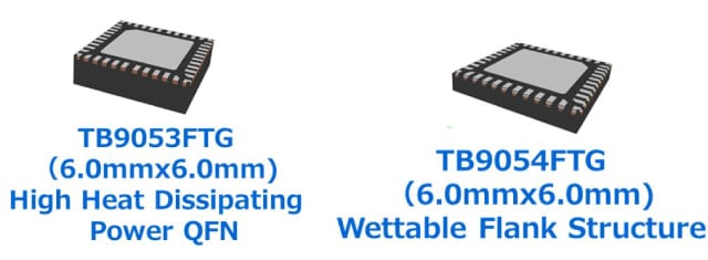
TB9053FTG/TB9054FTG utilize the same chip but employ different packages. Both packages are a small 6.0mmx6.0mm but are designed to be used differently depending on power consumption. If the current to be applied to the motor load is large, the TB9053FTG, which uses our original small footprint Power QFN package, is recommended. On the other hand, if power consumption is relatively low, the TB9054FTG, which uses a wettable flank structure for easy mounting, can be used. (See Figure 1)
TB9053FTG is a high heat-dissipating power package with a metal plate between the chip and the lead frame which suppresses transient heat rise by increasing thermal capacity. TB9054FTG has a wettable flank structure that leaves part of the terminal plated, improve mounting inspection and solder joint reliability.
Three types of motor connection output circuits can be configured
This product features a built-in 2-channel H-Bridge circuit, which can also be used as a 1-channel H-Bridge with double the current capability by externally shorting the driver output terminals (OUT1, OUT2 & OUT3, OUT4). To further expand the application, it can also be used as a 4-channel Half-Bridge. Figure 2 shows the block diagram and an example application circuit.
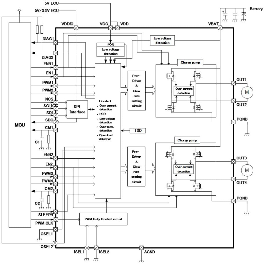
An example of a single product driving two bi-directional brushed motors. This product also has an abnormality detection function to enhance product and system safety.
Figure 3 also shows an image of the three types of output circuits and motor connections of this IC.
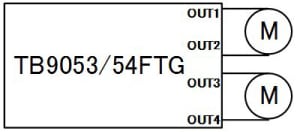
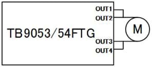
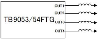
Figure 3: Three types of output circuits and motor connection images
This product covers a wide range of diverse applications. (1) example of driving two brushed motors (peak current 5A) bi-directionally with a 2-channel H-Bridge type driver. (2) example of driving one brush motor (peak current 10A) bi-directionally by shorting 2ch H-Bridge type driver to create 1 large ch. (3) example of driving a 4-channel Half-Bridge type motor with four brushes, an L-load, or a stepping motor with 2-phase excitation.
PWM drive is possible only by SPI communication
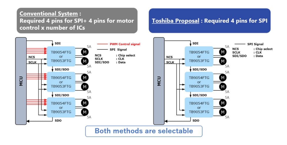
Normally, SPI communication has the function of informing the outside world of the internal settings and status of an IC. This product can also implement PWM of control of motors using only SPI communication. Normally, when controlling multiple motors, the number of ports on the MCU increases in proportion to the number of motors, potentially increasing, the required package size of the MCU to support the increase in the number of ports. However, the TB9053/54 products can generate PWM signals inside the IC, enabling motor control through only SPI communication connection, preventing the number of ports from increasing. In addition, this product supports daisy chain, which allows the MCU to be configured with fewer ports when many motors are used, thus contributing greatly to cost reductions.
Figures 4 and 5 illustrate this.
The left side is an example of a conventional PWM drive signal supplied from the MCU. The right side is an example driving with only SPI signals. PWM signals can be generated by SPI control using the internal clock signals of the integrated circuit (IC).
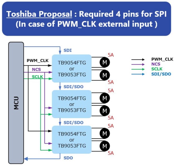
Figure 5 demonstrates how PWM control for applications which require high accuracy can be realized by using a high-precision clock signal from the MCU.
In-vehicle features and detection circuitry
Table 1 summarizes the key features and Table 2 summarizes the detection functions.
| Feature | Description | Control/Setup Method |
|---|---|---|
| Slew rate adjustment | Seven built-in slew rates | Set by SPI. |
| Current Limit | Chopping type current limit system. Two types of current limit values are also built in. | Change of current limit value is set by SPI. |
| Hi-side Current Monitor | Monitor 0.24% of the current flowing on the Hi-side | Insert a resistor between CMx pin[Note 1] and GND to convert current to voltage. |
| Sleep Mode | Standby current can be lowered. | Sleep terminal. |
| Diag Detection | Outputs a detection signal from the DIAGx pin[Note 1] when abnormality is detected. | Connect a pull-up resistor to the DIAGx pin.[Note 1] |
| Initial diagnostics check | Check the initial operation of each detection circuit for VBAT/VCC low voltage, overheat, overcurrent, and operating/non-operating load OPEN inside the IC. | Except for the load OPEN detection during non-operation, diagnostics are performed when the power is turned on or when the driver output is turned off with the ENx[Note1] /ENBx[Note 1] pins. Load OPEN detection during non-operation can be diagnosed by SPI indication. |
| Feature | Abnormality detection results confirmation method | Method of restoring abnormality detection results | |
|---|---|---|---|
| DIAGx terminal[Note 1] | SPI | ||
| VBAT Low voltage detection |
DIAGx terminal[Note 1] or SPI output pin (SDO) | automatic return | automatic return |
| VCC Low voltage detection |
DIAGx terminal[Note 1] or SPI output pin (SDO) | automatic return | Latched until 1WC[Note 2] is received |
| Overheat detection | DIAGx terminal[Note 1] or SPI output pin (SDO) | automatic return | automatic return |
| Supply/Ground fault detection[Note 3] | DIAGx terminal[Note 1] or SPI output pin (SDO) | Since these are latch type, ENx/ENBx[Note 1] pins need to be cleared. | Latch until 1WC[Note 2] is received, or automatic return is selectable via SPI |
| Load OPEN detection during operation[Note 4] | DIAGx terminal[Note 1] or SPI output pin (SDO) | automatic return | automatic return |
| Load OPEN detection during non-operation[Note 5] | DIAG terminal[Note 1] or SPI output pin (SDO) | automatic return | automatic return |
[Note 1] x represents a channel number of 1 or 2.
[Note 2] "1WC" means flag signal is cleared by writing once.
[Note 3] The state of the motor phase input is monitored by the voltage between the drain and source of the output MOS inside the IC.
[Note 4] The current flowing in the motor is monitored.
[Note 5] The current generated inside the IC is applied to the motor and monitored.
The TB9032 & TB9054 are new products that started mass-production in 2022. As the wave of electrification toward achieving carbon neutrality continues to grow, Toshiba will contribute to the automotive motor market by expanding our product lineup including gate driver products in as well as built-in driver products.
Related information
Follow the link below for more on Toshiba’s Automotive Brushed DC Motor Driver ICs.
Queries about purchasing, sampling and IC reliability
재고 확인 및 구매
3글자 이상 입력하세요.
Through this website you are able to proceed to the website of our distributors ("Third Party Website") which is not under the control of Toshiba Corporation and its subsidiaries and affiliates (collectively "Toshiba"). The Third Party Website is made available to you as a convenience only and you agree to use the Third Party Website at your own risk. The link of the Third Party Website does not necessarily imply a recommendation or an endorsement by Toshiba of the Third Party Website. Please be aware that Toshiba is not responsible for any transaction done through the Third Party Website, and such transactions shall be subject to terms and conditions which may be provided in the Third Party Website.
* Company names, product names, and service names may be trademarks of their respective companies.