- General Top
- SEMICONDUCTOR
- STORAGE
- COMPANY
-
My ToshibaSemicon
- Semiconductor Top
-
ApplicationsAutomotive
Body Electronics
xEV
In-Vehicle Infotainment
Advanced Driver-Assistance Systems (ADAS)
Chassis
IndustrialInfrastructure
BEMS/HEMS
Factory Automation
Commercial Equipment
Consumer/PersonalIoT Equipment
Healthcare
Wearable Device
Mobile
Computer Peripherals
-
ProductsAutomotive Devices
Discrete Semiconductor
Diodes
Transistors
Logic ICs
Analog Devices
- Automotive SmartMCD™ (Integreted SoC Conbining Microcontroller and Driver)
- Automotive Brushless Motor Driver ICs
- Automotive Brushed DC Motor Driver ICs
- Automotive Stepping Motor Driver ICs
- Automotive Driver ICs
- Automotive System Power Supplies ICs
- Automotive audio power amplifier ICs
- Automotive Network Communication
Digital Devices
Wireless Devices
※
 : Products list (parametric search)Power Semiconductors
SiC Power Devices
※
: Products list (parametric search)Isolators/Solid State RelaysPhotocouplers
Digital Isolators
Solid State Relays
Fiber Optic Transmitting Modules
※
: Products list (parametric search)MOSFETsIGBTs/IEGTsBipolar Transistors※
: Products list (parametric search)Diodes※
: Products list (parametric search)MicrocontrollersMotor Driver ICsIntelligent Power ICs※
: Products list (parametric search)Power Management ICsLinear ICs※
: Products list (parametric search)General Purpose Logic ICsLinear Image SensorsOther Product ICsOther Product ICs
※
: Products list (parametric search) -
Design & Development
Design & Development
Innovation Centre
At the Toshiba Innovation Centre we constantly strive to inspire you with our technologies and solutions. Discover how to place us at the heart of your innovations.
-
Knowledge
Knowledge
Highlighted Topics
Further Materials
Other
- Where To Buy


- Part Number & Keyword Search
- Cross Reference Search
- Parametric Search
- Stock Check & Purchase
This webpage doesn't work with Internet Explorer. Please use the latest version of Google Chrome, Microsoft Edge, Mozilla Firefox or Safari.
require 3 characters or more. Search for multiple part numbers fromhere.
The information presented in this cross reference is based on TOSHIBA's selection criteria and should be treated as a suggestion only. Please carefully review the latest versions of all relevant information on the TOSHIBA products, including without limitation data sheets and validate all operating parameters of the TOSHIBA products to ensure that the suggested TOSHIBA products are truly compatible with your design and application.Please note that this cross reference is based on TOSHIBA's estimate of compatibility with other manufacturers' products, based on other manufacturers' published data, at the time the data was collected.TOSHIBA is not responsible for any incorrect or incomplete information. Information is subject to change at any time without notice.
require 3 characters or more.
Do bidirectional bus buffers have any constraints on the timing of the direction (DIR), bus, and other signals?
This device can easily achieve bidirectional switching, but care must be taken for bus buffer output conflicts and input floating.
Although this bus buffer allows the signal direction to be switched easily, the following considerations apply:
- Ensure that the outputs of the bus buffer do not enter into conflict with the outputs of other buffers when DIR changes state.
→ A conflict causes not only an abnormal output condition but also excessive current, possibly damaging these devices. - Ensure that the inputs do not float (i.e., are not left open or in the High-Z state).
→ A floating input is easily affected by electromagnetic susceptibility (EMS) and might cause an abnormal output condition or output oscillation as parasitic capacitances are charged by leakage current.
Fig. 1 shows the equivalent circuit of the bi-directional bus buffer (74VHC245), and Table-1 shows the truth table.
When /G is "H" level, all input/output terminals are floating, so it is necessary to pull up to the power supply or pull down to GND.
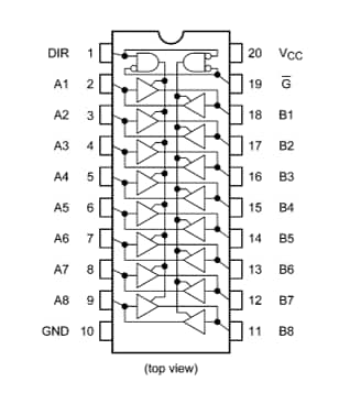
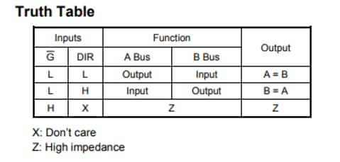
Table-1 Truth table of Bi-directional bus buffer (74VHC245)
The following describes the timing requirements using the circuit and timing diagrams as shown in Fig. 2.
A bidirectional bus buffer is connected between the A bus and the B bus. In the initial state, the A pin is an input, and the B pin is an output. Therefore, a signal is transmitted from the A bus to the B bus. At this time, Buffer Y is disabled (i.e., provides no output).

- Disable the bidirectional bus buffer by setting the /G pin High. It takes a period of tpLZ for the bus buffer to be disabled. Then, the A and B pins assume the Hi-Z state. It is therefore necessary to stabilize their potential by connecting, for example, pull-up resistors (Rpullup1 and Rpullup2) to these pins. Bus buffers with a bushold capability do not require any pull-up resistors.
- The output enters into a conflict after the signal direction changes. Therefore, disable the output of Buffer X and enable the output of Buffer Y while the bus buffer is disabled. Also, set the direction pin (DIR) from Low to High during this period.
- Enable the bus buffer by setting the /G pin Low.
The internal circuit changes its mode while the DIR pin changes state (from Low to High or High to Low) and while the enable pin (/G or /OE) changes state. During these periods, the output value is indeterminate, meaning it cannot be determined whether the output is High, Low, or between High and Low. Take this into consideration when creating a design since the output value during these periods cannot be guaranteed.
Related Links
The following documents also contain related information.