
-
My ToshibaSemicon
- 반도체 탑
-
애플리케이션Automotive
Body Electronics
xEV
In-Vehicle Infotainment
Advanced Driver-Assistance Systems (ADAS)
Chassis
IndustrialInfrastructure
BEMS/HEMS
Factory Automation
Commercial Equipment
Consumer/PersonalIoT Equipment
Healthcare
Wearable Device
Mobile
Computer Peripherals
-
제품자동차 디바이스
Discrete Semiconductor
다이오드
트랜지스터
로직 IC
Analog Devices
Digital Devices
Wireless Devices
※
 : Products list (parametric search)파워반도체
※
: Products list (parametric search)Isolators/Solid State RelaysPhotocouplers
Digital Isolators
Solid State Relays
Fiber Optic Transmitting Modules
※
: Products list (parametric search)MOSFETsIGBTs/IEGTs바이폴라 트랜지스터※
: Products list (parametric search)다이오드※
: Products list (parametric search)마이크로컨트롤러모터 드라이버 ICIntelligent Power ICs※
: Products list (parametric search)전원관리IC리니어 IC※
: Products list (parametric search)범용로직IC리니어 이미지 센서기타 제품용 IC기타 제품용 IC
※
: Products list (parametric search) -
개발/설계 지원
-
기술 자료
- 구매처


- 부품 번호 & 키워드 검색
- 상호 참조 검색
- 파라미터 검색
- 재고 확인 및 구매
This webpage doesn't work with Internet Explorer. Please use the latest version of Google Chrome, Microsoft Edge, Mozilla Firefox or Safari.
3글자 이상 입력하세요. Search for multiple part numbers fromhere.
The information presented in this cross reference is based on TOSHIBA's selection criteria and should be treated as a suggestion only. Please carefully review the latest versions of all relevant information on the TOSHIBA products, including without limitation data sheets and validate all operating parameters of the TOSHIBA products to ensure that the suggested TOSHIBA products are truly compatible with your design and application.Please note that this cross reference is based on TOSHIBA's estimate of compatibility with other manufacturers' products, based on other manufacturers' published data, at the time the data was collected.TOSHIBA is not responsible for any incorrect or incomplete information. Information is subject to change at any time without notice.
3글자 이상 입력하세요.
High withstand voltage (reverse voltage) characteristics of SiC SBDs
Silicon carbide (SiC) is a wide-bandgap semiconductor with a bandgap of 3.26 eV, much higher than that of silicon (Si) (=1.12 eV). SiC provides high electric breakdown field and high thermal conductivity because of high atomic bond due to a low lattice constant (i.e., a short atom-to-atom distance).
Comparisons of physical properties between Si and SiC
| Characteristics | Unit | Si | 4H-SiC |
|---|---|---|---|
| Bandgap | eV | 1.12 | 3.26 |
| Electron mobility, μe | cm2/Vs | 1400 | 1000/1200 |
| Hole mobility, μh | 600 | 120 | |
| Electric breakdown field, Ec | V/cm | 3.0×10⁵ | 2.8×10⁶ |
| Thermal conductivity, λ | W/cmK | 1.5 | 4.9 |
| Saturation electron drift velocity, Vsat | cm/s |
1.0×10⁷ | 2.2×10⁷ |
| Relative dielectric constant, ε | 11.8 | 9.7/10.2 |
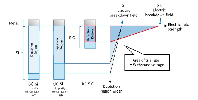
When an SBD with a conventional structure is reverse-biased, the depletion region extends into the semiconductor as shown below. The area of the triangle formed by the electric breakdown field and the depletion region width represents the withstand voltage of an SBD. The depletion region depth is inversely proportional to the dopant concentration. Increasing the dopant concentration helps reduce the resistance of silicon and therefore the forward voltage (VF) of the SBD, but at the expense of withstand voltage (i.e., triangle area). The electric breakdown field of SiC is nearly 10 times that of silicon. As shown below, it is therefore possible to increase the withstand voltage (i.e., triangle area) of a SiC SBD relative to a Si SBD, even if it is heavily doped.
In addition, since the depletion layer is less stretched by the higher concentration, the thickness of the chip can be thinner than in the case of Si. The thickness of the semiconductor (Si or SiC) can be considered as series resistance in the forward direction, and so the forward voltage can be improved by reducing the thickness.
SiC schottky barrier diodes
Related information
Queries about purchasing, sampling and IC reliability
재고 확인 및 구매
3글자 이상 입력하세요.
Through this website you are able to proceed to the website of our distributors ("Third Party Website") which is not under the control of Toshiba Corporation and its subsidiaries and affiliates (collectively "Toshiba"). The Third Party Website is made available to you as a convenience only and you agree to use the Third Party Website at your own risk. The link of the Third Party Website does not necessarily imply a recommendation or an endorsement by Toshiba of the Third Party Website. Please be aware that Toshiba is not responsible for any transaction done through the Third Party Website, and such transactions shall be subject to terms and conditions which may be provided in the Third Party Website.