
- 半導體首頁
-
應用Automotive
Body Electronics
xEV
In-Vehicle Infotainment
Advanced Driver-Assistance Systems (ADAS)
Chassis
IndustrialInfrastructure
BEMS/HEMS
Factory Automation
Commercial Equipment
Consumer/PersonalIoT Equipment
Healthcare
Wearable Device
Mobile
Computer Peripherals
-
產品車用元件
Discrete Semiconductor
Diodes
電晶體
通用邏輯IC
Analog Devices
Digital Devices
Wireless Devices
※
 : Products list (parametric search)功率半導體
※
: Products list (parametric search)隔離器/固態繼電器Photocouplers
Digital Isolators
※
: Products list (parametric search)MOSFETsIGBTs/IEGTs雙極性電晶體※
: Products list (parametric search)Diodes※
: Products list (parametric search)微控制器馬達驅動 ICs智能功率 ICs※
: Products list (parametric search)電源管理 ICs線性 ICs※
: Products list (parametric search)通用邏輯 ICs線性影像感測器其他產品其他產品
※
: Products list (parametric search) -
開發/設計支援
開發 / 設計支援
-
技術知識
- 購買管道


- 型號 & 關鍵字搜尋
- 交叉搜尋
- 參數搜尋
- 線上庫存查詢跟購買
This webpage doesn't work with Internet Explorer. Please use the latest version of Google Chrome, Microsoft Edge, Mozilla Firefox or Safari.
型號需要超過三個文字以上 Search for multiple part numbers fromhere.
The information presented in this cross reference is based on TOSHIBA's selection criteria and should be treated as a suggestion only. Please carefully review the latest versions of all relevant information on the TOSHIBA products, including without limitation data sheets and validate all operating parameters of the TOSHIBA products to ensure that the suggested TOSHIBA products are truly compatible with your design and application.Please note that this cross reference is based on TOSHIBA's estimate of compatibility with other manufacturers' products, based on other manufacturers' published data, at the time the data was collected.TOSHIBA is not responsible for any incorrect or incomplete information. Information is subject to change at any time without notice.
型號需要超過三個文字以上
High withstand voltage (reverse voltage) characteristics of SiC SBDs
Silicon carbide (SiC) is a wide-bandgap semiconductor with a bandgap of 3.26 eV, much higher than that of silicon (Si) (=1.12 eV). SiC provides high electric breakdown field and high thermal conductivity because of high atomic bond due to a low lattice constant (i.e., a short atom-to-atom distance).
Comparisons of physical properties between Si and SiC
| Characteristics | Unit | Si | 4H-SiC |
|---|---|---|---|
| Bandgap | eV | 1.12 | 3.26 |
| Electron mobility, μe | cm2/Vs | 1400 | 1000/1200 |
| Hole mobility, μh | 600 | 120 | |
| Electric breakdown field, Ec | V/cm | 3.0×10⁵ | 2.8×10⁶ |
| Thermal conductivity, λ | W/cmK | 1.5 | 4.9 |
| Saturation electron drift velocity, Vsat | cm/s |
1.0×10⁷ | 2.2×10⁷ |
| Relative dielectric constant, ε | 11.8 | 9.7/10.2 |
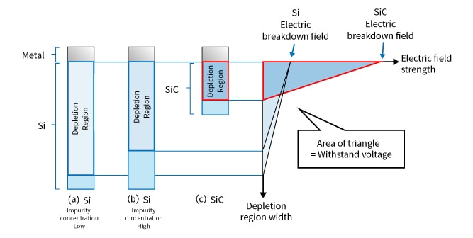
When an SBD with a conventional structure is reverse-biased, the depletion region extends into the semiconductor as shown below. The area of the triangle formed by the electric breakdown field and the depletion region width represents the withstand voltage of an SBD. The depletion region depth is inversely proportional to the dopant concentration. Increasing the dopant concentration helps reduce the resistance of silicon and therefore the forward voltage (VF) of the SBD, but at the expense of withstand voltage (i.e., triangle area). The electric breakdown field of SiC is nearly 10 times that of silicon. As shown below, it is therefore possible to increase the withstand voltage (i.e., triangle area) of a SiC SBD relative to a Si SBD, even if it is heavily doped.
In addition, since the depletion layer is less stretched by the higher concentration, the thickness of the chip can be thinner than in the case of Si. The thickness of the semiconductor (Si or SiC) can be considered as series resistance in the forward direction, and so the forward voltage can be improved by reducing the thickness.
SiC schottky barrier diodes
Related information
Queries about purchasing, sampling and IC reliability
線上庫存查詢跟購買
型號需要超過三個文字以上
Through this website you are able to proceed to the website of our distributors ("Third Party Website") which is not under the control of Toshiba Corporation and its subsidiaries and affiliates (collectively "Toshiba"). The Third Party Website is made available to you as a convenience only and you agree to use the Third Party Website at your own risk. The link of the Third Party Website does not necessarily imply a recommendation or an endorsement by Toshiba of the Third Party Website. Please be aware that Toshiba is not responsible for any transaction done through the Third Party Website, and such transactions shall be subject to terms and conditions which may be provided in the Third Party Website.