
-
My ToshibaSemicon
- 반도체 탑
-
애플리케이션Automotive
Body Electronics
xEV
In-Vehicle Infotainment
Advanced Driver-Assistance Systems (ADAS)
Chassis
IndustrialInfrastructure
BEMS/HEMS
Factory Automation
Commercial Equipment
Consumer/PersonalIoT Equipment
Healthcare
Wearable Device
Mobile
Computer Peripherals
-
제품자동차 디바이스
Discrete Semiconductor
다이오드
트랜지스터
로직 IC
Analog Devices
Digital Devices
Wireless Devices
※
 : Products list (parametric search)파워반도체
※
: Products list (parametric search)Isolators/Solid State RelaysPhotocouplers
Digital Isolators
Solid State Relays
Fiber Optic Transmitting Modules
※
: Products list (parametric search)MOSFETsIGBTs/IEGTs바이폴라 트랜지스터※
: Products list (parametric search)다이오드※
: Products list (parametric search)마이크로컨트롤러모터 드라이버 ICIntelligent Power ICs※
: Products list (parametric search)전원관리IC리니어 IC※
: Products list (parametric search)범용로직IC리니어 이미지 센서기타 제품용 IC기타 제품용 IC
※
: Products list (parametric search) -
개발/설계 지원
-
기술 자료
- 구매처


- 부품 번호 & 키워드 검색
- 상호 참조 검색
- 파라미터 검색
- 재고 확인 및 구매
This webpage doesn't work with Internet Explorer. Please use the latest version of Google Chrome, Microsoft Edge, Mozilla Firefox or Safari.
3글자 이상 입력하세요. Search for multiple part numbers fromhere.
The information presented in this cross reference is based on TOSHIBA's selection criteria and should be treated as a suggestion only. Please carefully review the latest versions of all relevant information on the TOSHIBA products, including without limitation data sheets and validate all operating parameters of the TOSHIBA products to ensure that the suggested TOSHIBA products are truly compatible with your design and application.Please note that this cross reference is based on TOSHIBA's estimate of compatibility with other manufacturers' products, based on other manufacturers' published data, at the time the data was collected.TOSHIBA is not responsible for any incorrect or incomplete information. Information is subject to change at any time without notice.
3글자 이상 입력하세요.
3-1 Key characteristics for normal operation (in the absence of an ESD event)(2)
3-1(2) Whether the total capacitance (Ct) of an ESD protection diode is sufficiently low with respect to the frequency of the signal line to be protected
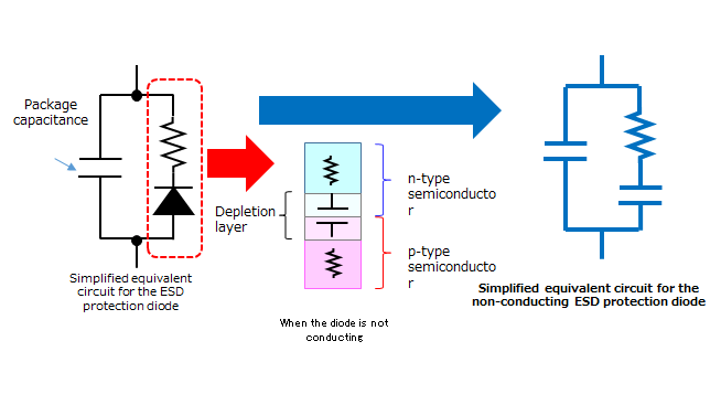
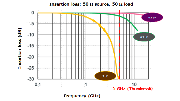
Figure 3.3 shows an equivalent circuit of an ESD protection diode. The diode does not conduct during normal operation. At this time, a depletion layer is formed at the interface of the pn junction as shown in Figure 3.3. The depletion layer electrically acts as a capacitor. Therefore, the signal quality is degraded unless appropriate ESD protection diodes are selected, considering the frequency of the signal lines to be protected. Figure 3.4 shows the insertion loss characteristics of ESD protection diodes with a total capacitance (CT) of 5 pF, 0.3 pF, and 0.1 pF. Diodes with a larger capacitance cause higher insertion loss (as indicated by a larger negative change in the characteristics curve), restricting the frequency range in which they can be used. For example, in the case of Thunderbolt (with a bandwidth of 10 Gbps, which is equivalent to a frequency of 5 GHz), ESD protection diodes with a small capacitance (0.1 to 0.3 pF) cause a small insertion loss and hardly affect the signal passing through the diode whereas an ESD protection diode with a capacitance of 5 pF causes a large insertion loss, considerably decaying the signal that passes through the diode.
Reduction in total capacitance
(Total capacitance consists of the junction capacitance of a diode and the parasitic capacitance of the package in which it is housed.
The junction capacitance constitutes a large proportion of a diode’s total capacitance.)
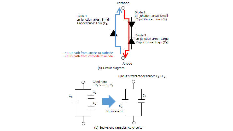
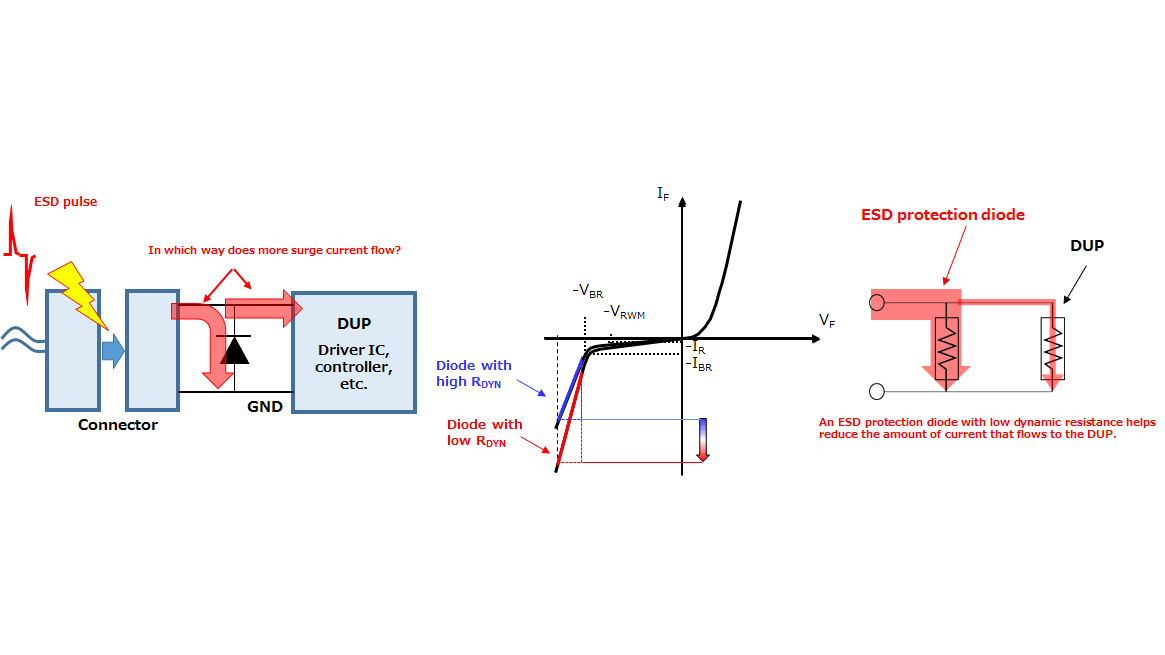
A diode has capacitance because of the depletion layer that is formed across the pn junction (p: p-type semiconductor, n: n-type semiconductor) when it is reverse-biased. In contrast to the capacitance, the depletion layer acts as an insulating layer where minority carriers do not exist. Reducing the dopant concentration of the semiconductor regions causes an increase in the width of the depletion layer. Therefore, in order to reduce the capacitance of a diode, it is necessary to reduce the area of the pn junction or increase the reverse breakdown voltage (VBR), but either way results in the degradation of its ESD immunity. When two diodes are connected in series, their combined capacitance decreases. Also, diodes are less tolerant of ESD energy in the reverse direction than in the forward direction. Toshiba’s low-capacitance (Ct) ESD protection diodes are fabricated using a process called the ESD diode array process (EAP), which combines multiple diodes to reduce capacitance without compromising the ESD immunity.
Figure 3.5 shows the circuit diagram of a low-capacitance ESD protection diode in an EAP configuration. It consists of three diodes: low-capacitance Diode 1 and Diode 2 (with a capacitance of C1 and C2 respectively) and high-capacitance Diode 3 (with a capacitance of C3). Diode 1 and Diode 2 have a small pn junction area and high VBR whereas Diode 3 has a large pn junction area and adequate VBR. The ESD current applied to the anode flows through Diode 1 in the forward direction whereas the one applied to the cathode flows through Diode 2 in the forward direction and then through Diode 3 in the reverse direction since the VBR of Diode 3 is lower than that of Diode 1. Typically, diodes are less tolerant of ESD energy in the reverse direction than in the forward direction. Since the pn junction area of Diode 1 and Diode 2 is small, they are even less tolerant of ESD energy in the reverse direction. However, when an ESD protection diode is configured as shown in Figure 3.5(a), ESD current does not flow through Diode 1 and Diode 2 in the reverse direction. Therefore, this circuit provides high ESD immunity as a whole. Figure 3.5(b) shows the equivalent capacitance circuit of this ESD protection diode. The combined capacitance can be reduced by connecting low-capacitance Diode 2 and high-capacitance Diode 3 in series. Also, since the VBR of this circuit is determined by the VBR of Diode 3, ESD immunity can be increased by adjusting the VBR of Diode 3 according to the signal line to be protected.
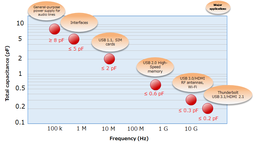
Rough total capacitance versus signal frequency
Figure 3.6 can be used as guide when selecting ESD protection diodes according to the signal frequency.
3 Key electrical characteristics of TVS diodes (ESD protection diodes)


- 1 What is a TVS diode (ESD protection diode)?
- 2 Basic operations of TVS diodes (ESD protection diodes)
- 4 Selection guidelines for TVS diodes (ESD protection diodes)
- 5 Layout considerations for TVS diodes (ESD protection diodes)
- 6 Absolute maximum ratings of TVS diodes (ESD protection diodes)
- 7 Electrical characteristics of TVS diodes (ESD protection diodes)
Related information
- Product Web Page
TVS Diodes (ESD protection diodes) - Applidcation Notes
Diode - FAQ
TVS diodes (ESD protection diodes) - Parametric searches for all Toshiba TVS diode (ESD protection diodes) produ cts are available here:
Parametric search - Stock Check & Purchase Toshiba TVS diode (ESD protection diodes) here
Stock Check & Purchase