
-
My ToshibaSemicon
- 반도체 탑
-
애플리케이션Automotive
Body Electronics
xEV
In-Vehicle Infotainment
Advanced Driver-Assistance Systems (ADAS)
Chassis
IndustrialInfrastructure
BEMS/HEMS
Factory Automation
Commercial Equipment
Consumer/PersonalIoT Equipment
Healthcare
Wearable Device
Mobile
Computer Peripherals
-
제품자동차 디바이스
Discrete Semiconductor
다이오드
트랜지스터
로직 IC
Analog Devices
Digital Devices
Wireless Devices
※
 : Products list (parametric search)파워반도체
※
: Products list (parametric search)Isolators/Solid State RelaysPhotocouplers
Digital Isolators
Solid State Relays
Fiber Optic Transmitting Modules
※
: Products list (parametric search)MOSFETsIGBTs/IEGTs바이폴라 트랜지스터※
: Products list (parametric search)다이오드※
: Products list (parametric search)마이크로컨트롤러모터 드라이버 ICIntelligent Power ICs※
: Products list (parametric search)전원관리IC리니어 IC※
: Products list (parametric search)범용로직IC리니어 이미지 센서기타 제품용 IC기타 제품용 IC
※
: Products list (parametric search) -
개발/설계 지원
-
기술 자료
- 구매처


- 부품 번호 & 키워드 검색
- 상호 참조 검색
- 파라미터 검색
- 재고 확인 및 구매
This webpage doesn't work with Internet Explorer. Please use the latest version of Google Chrome, Microsoft Edge, Mozilla Firefox or Safari.
3글자 이상 입력하세요. Search for multiple part numbers fromhere.
The information presented in this cross reference is based on TOSHIBA's selection criteria and should be treated as a suggestion only. Please carefully review the latest versions of all relevant information on the TOSHIBA products, including without limitation data sheets and validate all operating parameters of the TOSHIBA products to ensure that the suggested TOSHIBA products are truly compatible with your design and application.Please note that this cross reference is based on TOSHIBA's estimate of compatibility with other manufacturers' products, based on other manufacturers' published data, at the time the data was collected.TOSHIBA is not responsible for any incorrect or incomplete information. Information is subject to change at any time without notice.
3글자 이상 입력하세요.
What is an IGBT?
An IGBT (Insulated Gate Bipolar Transistor) is a power device that combines the high input impedance of a MOSFET with the low on-state voltage characteristics of a bipolar transistor (BJT). It is suitable for high-voltage and high-current applications and is used in a wide range of products, from home appliances to industrial equipment.
Basic Structure and Operation
An IGBT consists of a MOSFET structure on the input side and a bipolar transistor (BJT) structure on the output side.
When a voltage is applied to the gate, the MOSFET portion turns on, and current flows between the collector and emitter.
Figure 1 shows the symbol of an N-channel IGBT. Figure 2 shows the equivalent circuit of an N-channel IGBT.
The reasons why an IGBT can handle large current and how carriers behave inside the device (conductivity modulation) are explained in later sections.
For additional information on operating principles, refer to the following FAQ:
> What is the principle of operation of the IGBT?

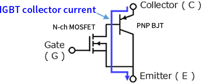
Figure 1 Notes
Figure 1 shows the circuit symbol of an N-channel IGBT. The gate is drawn as a vertical line separated from the other terminal lines, indicating that the gate is electrically insulated from the other terminals. The arrows associated with the collector and emitter indicate the direction of current flow. The vertical line drawn between the collector and emitter symbolically indicates that a current path is formed by MOSFET gate control and does not represent the physical channel structure inside the device.
Figure 2 Notes
Figure 2 shows the equivalent circuit of an N-channel IGBT. The device is represented as a combination of an N-channel MOSFET and a PNP bipolar transistor (BJT). The blue solid line indicates the main current path in the on-state. The external collector terminal corresponds to the p+ layer on the backside of the chip (the emitter side of the PNP BJT), and current flows to the emitter through the MOSFET section. This equivalent circuit representation illustrates the combined operation of the MOSFET and the BJT in the IGBT.
Comparison of MOSFETs, BJTs, and IGBTs
IGBTs are designed to combine the advantages of MOSFETs and BJTs, as shown in the following comparison.
- MOSFET characteristics:
- High input impedance
- Fast switching speed
- However, when designed for higher breakdown voltages, on-resistance tends to increase
- BJT characteristics:
- Low on-state voltage and low conduction loss
- However, input impedance is low and switching tends to be slow
- IGBT characteristics:
- High input impedance
- Switching is slower than that of MOSFETs, but relatively fast
- Low on-state voltage even at high breakdown voltage ratings
Because of these characteristics, IGBTs are widely adopted in consumer products such as air conditioners, refrigerators, washing machines, and microwave ovens, as well as industrial equipment such as elevators, robots, and machine tools.
IGBT Structure
An IGBT is a vertical power device that combines a MOSFET structure with a bipolar transistor (BJT) structure.
When a channel is formed in the MOSFET portion by the gate voltage, current flows between the collector and emitter.
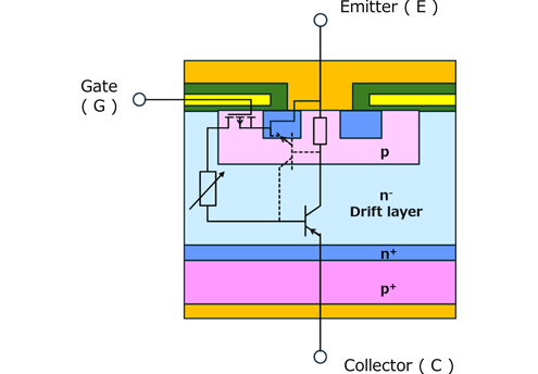
Figure 3 shows the overall structure of an N-channel IGBT, and Figure 4 shows the equivalent circuit corresponding to that structure.
A typical IGBT structure is a vertical structure in which a p+ layer is added beneath the drift region (n− layer) of a lateral MOSFET. This p+ layer functions as the external collector.
Figure 4 shows an equivalent circuit derived from the basic device structure. This equivalent circuit includes parasitic NPN bipolar transistors that are not included in simplified equivalent circuit models. These parasitic elements form a thyristor structure.
Latch-up resulting from this structure is described later.
Electrons flow into the n− layer through the channel formed near the drain side (chip surface), and holes are injected from the p+ layer side. This creates a bipolar current path that differs from a unipolar MOSFET.
This vertical layer structure is the basis for why IGBTs are suitable for high-voltage and high-current applications.
For additional information on IGBT structure, refer to the following e-learning content:
> 3-18. Performance Improvement of IGBTs: Evolution of Vertical Design
For the structure of an RC-IGBT (reverse-conducting IGBT) with a freewheeling diode integrated between the emitter and collector, refer to:
> What is a reverse-conducting IGBT (RC-IGBT)?

Parasitic Thyristor Structure and Latch-up
As shown in Figure 4, parasitic NPN and PNP transistors exist inside an IGBT, resulting in a thyristor structure.
If this parasitic thyristor turns on due to heat or abnormal conditions, latch-up can occur, and the collector–emitter path can become nearly short-circuited. This may lead to destruction due to overcurrent.
However, the base–emitter resistance of the parasitic NPN transistor (p-region resistance) is designed to be very small, which suppresses active turn-on of the parasitic NPN transistor. Therefore, modern IGBTs are structured such that latch-up rarely occurs.
Conductivity Modulation
In MOSFETs, increasing the breakdown voltage generally results in higher on-resistance.
Conductivity modulation is a mechanism used in IGBTs to suppress this increase in on-resistance under high-voltage conditions.
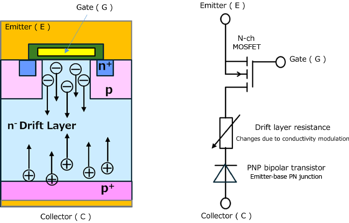
Most of the collector current in an IGBT flows from the emitter of the PNP BJT (the IGBT collector) to the base. This current passes through the drift region (n− layer), goes through the MOSFET drain–source path, and reaches the IGBT emitter. This is the main current path in an IGBT.
The resistance of the drift region is reduced by conductivity modulation. Conductivity modulation is a characteristic common to bipolar devices such as pn-junction diodes and BJTs, and it does not occur in unipolar devices such as MOSFETs and Schottky barrier diodes (SBDs).
When the IGBT turns on, a large number of holes are injected from the p+ collector layer into the n− drift layer. To maintain charge neutrality, electrons are also injected from the n+ layer side through the MOSFET channel. As a result, the carrier density of both electrons and holes increases significantly in the n− layer (high-level injection), improving conductivity.
In other words, conductivity modulation is the phenomenon in which the resistance of the n− layer decreases as both electrons and holes increase.
Figure 5 shows carrier operation during conductivity modulation and an equivalent circuit representation.
In this figure, the PNP BJT connected to the external collector terminal (C) is represented as a diode, and the drift-region resistance that changes due to conductivity modulation is represented as a variable resistor.
Tail Current
When an IGBT transitions from on to off, the gate–emitter terminals are short-circuited or reverse-biased. This discharges the gate charge and eliminates the channel, turning off the MOSFET portion.
However, the collector current does not immediately stop and continues to flow for a while as tail current. This tail current occurs because excess electrons and holes stored in the n− drift layer during conductivity modulation remain, and current continues to flow while these carriers recombine and disappear.
Tail current affects switching loss and is an important consideration in circuit design.
For additional information, refer to the following FAQs:
> Conductivity modulation: What is conductivity modulation?
> Tail current: What is the tail current of an IGBT?
Related Links
The following documents also contain related information.
파라미터 검색
IGBT/IEGT
자주 있는 문의
* Company names, product names, and service names used in this FAQ may be of their respective companies.