-
My ToshibaSemicon
- 반도체 탑
-
애플리케이션Automotive
Body Electronics
xEV
In-Vehicle Infotainment
Advanced Driver-Assistance Systems (ADAS)
Chassis
IndustrialInfrastructure
BEMS/HEMS
Factory Automation
Commercial Equipment
Consumer/PersonalIoT Equipment
Healthcare
Wearable Device
Mobile
Computer Peripherals
-
제품자동차 디바이스
Discrete Semiconductor
다이오드
트랜지스터
로직 IC
Analog Devices
Digital Devices
Wireless Devices
※
: Products list (parametric search)
파워반도체※
: Products list (parametric search)
Isolators/Solid State RelaysPhotocouplers
Digital Isolators
Solid State Relays
Fiber Optic Transmitting Modules
※
: Products list (parametric search)
MOSFETsIGBTs/IEGTs바이폴라 트랜지스터※
: Products list (parametric search)
다이오드※
: Products list (parametric search)
마이크로컨트롤러모터 드라이버 ICIntelligent Power ICs※
: Products list (parametric search)
전원관리IC리니어 IC※
: Products list (parametric search)
범용로직IC리니어 이미지 센서기타 제품용 IC기타 제품용 IC
※
: Products list (parametric search)
-
개발/설계 지원
-
기술 자료
- 구매처
- 부품 번호 & 키워드 검색
- 상호 참조 검색
- 파라미터 검색
- 재고 확인 및 구매
This webpage doesn't work with Internet Explorer. Please use the latest version of Google Chrome, Microsoft Edge, Mozilla Firefox or Safari.
3글자 이상 입력하세요. Search for multiple part numbers fromhere.
The information presented in this cross reference is based on TOSHIBA's selection criteria and should be treated as a suggestion only. Please carefully review the latest versions of all relevant information on the TOSHIBA products, including without limitation data sheets and validate all operating parameters of the TOSHIBA products to ensure that the suggested TOSHIBA products are truly compatible with your design and application.Please note that this cross reference is based on TOSHIBA's estimate of compatibility with other manufacturers' products, based on other manufacturers' published data, at the time the data was collected.TOSHIBA is not responsible for any incorrect or incomplete information. Information is subject to change at any time without notice.
3글자 이상 입력하세요.
High accurate SPICE model for medium to high voltage MOSFET (400V-900V)
Structure and features
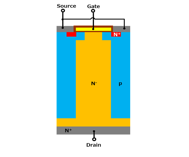
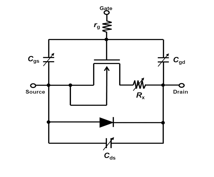
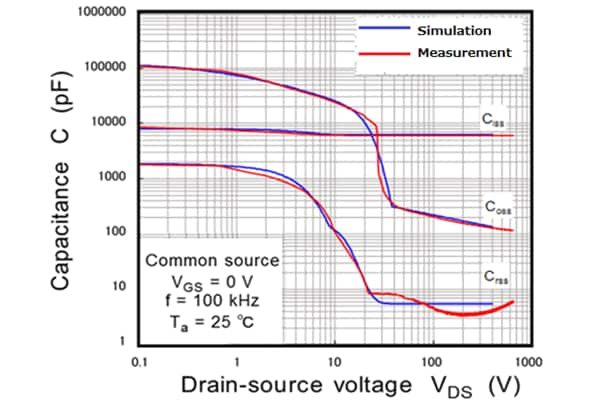
As shown in Fig. 1, Toshiba’s DTMOS series applies Superjunction (SJ) structure in which P and N layers are alternately arranged in the drift layer. The high accurate SPICE model (G2 model) for SJ structure MOSFET (SJ-MOSFET) developed by Toshiba can express the saturation characteristics in the high current region of Drain current vs Drain-source Voltage (ID-VDS) charactaristics. And the abrupt capacitance change depending on the MOSFET Drain voltage shown in Fig. 2 is also reproduced by using the arbitrary function.
MOSFET fitting accuracy
Fig. 3 shows the reproduction level (called "fitting accuracy") by comparing the actual measurement of ID-VGS characteristics and ID-VDS characteristics of our SJ-MOSFET product TK040N65Z with the simulation using our SPICE model. In the High voltage breakdown MOSFET such as SJ-MOSFET, Drain Current (ID) saturate due to the resistance effected by the deep and long drift layer. In our SPICE model, this saturation characteristic is expressed by a non-linear resister (RX) which applied to the drain side so the simulation curve can show actual measurement with accuracy even in the high current region.
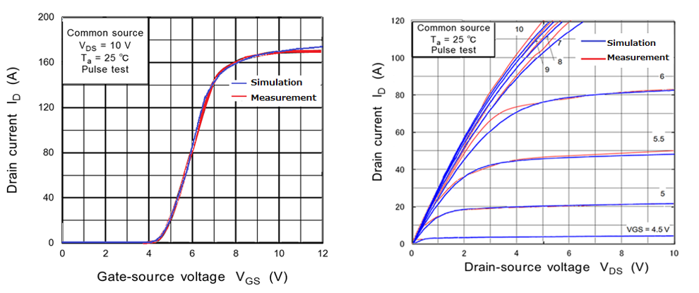
Fig. 4 shows a comparison between actual measurement and simulation of the VDS dependencies on the Input capacitance (Ciss), the Output capacitance (Coss), and the Reverse transfer capacitance (Crss). The capacitance characteristics of SJ-MOSFET change rapidly with the depletion layer extending from the PN-junction due to the SJ structure. On the other hand, Toshiba's SPICE model can show the non-linearity of the measurement values with high accuracy by additional arbitrary functions of non-linear capacitance combination of Gate-souece (Cgs), Gate-drain (Cgd) and Drain-source (Cds).
Transient characteristics (inductance load switching operation) fitting accuracy
Fig. 5 shows a inductive load switching circuit diagram using SJ-MOSFET product TK040N65Z. And Fig. 6 shows the comparison between the actual waveform and the simulation using the G2 model for SJ-MOSFET as described above. By using our G2 model which can express the non-linearity of the capacitance characteristic with high accuracy, we can see very accurate waveforms that the rising of VDS and oscillation of VDS and ID, associated with oscillation of dVDS/dt or VGS. Our G2 model for SJ-MOSFET is a SPICE model that can sufficiently verify dynamic properties such as switching operation.
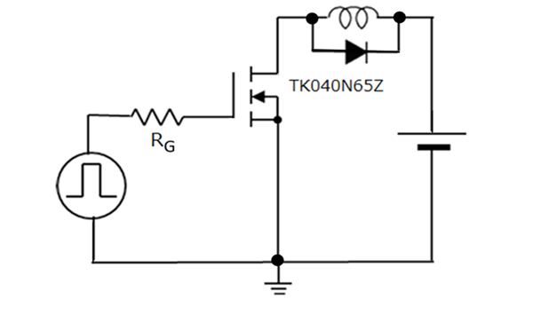
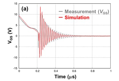
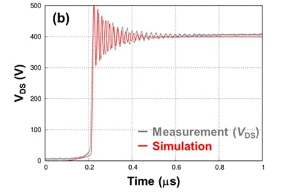
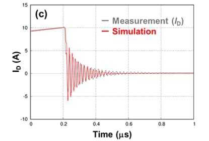
Fig. 6: Comparison of actual measurement and simulation of turn-off waveforms in inductance load switching circuit
(a)VGS (b)VDS (c)ID
Our high accurate SPICE model (G2 model) can reproduce the actual switching waveforms with high accuracy. The circuit verification by using high-accuracy simulation in advance of the actual production may reduce the double work for the circuit modification and help the development time shorten. Toshiba's high accurate SPICE model (G2 model) supports your circuit development and analysis effectively.

