
-
My ToshibaSemicon
- 홈페이지 보기
-
반도체 보기
-
애플리케이션
Body Electronics
xEV
In-Vehicle Infotainment
Advanced Driver-Assistance Systems (ADAS)
Chassis
Infrastructure
BEMS/HEMS
Factory Automation
Commercial Equipment
IoT Equipment
Healthcare
Wearable Device
Mobile
Computer Peripherals
-
제품
Discrete Semiconductor
다이오드
트랜지스터
로직 IC
Analog Devices
Digital Devices
Wireless Devices
※
 : Products list (parametric search)
※
: Products list (parametric search)Photocouplers
Digital Isolators
Solid State Relays
Fiber Optic Transmitting Modules
※
: Products list (parametric search)※
: Products list (parametric search)※
: Products list (parametric search)※
: Products list (parametric search)※
: Products list (parametric search)기타 제품용 IC
※
: Products list (parametric search) -
개발/설계 지원
-
기술 자료
- 구매처 보기
-
- 스토리지 보기
- 회사 개요 보기


- 부품 번호 검색
- 상호 참조 검색
- 키워드 검색
- 파라미터 검색
- 재고 확인 및 구매
This webpage doesn't work with Internet Explorer. Please use the latest version of Google Chrome, Microsoft Edge, Mozilla Firefox or Safari.
3글자 이상 입력하세요.
The information presented in this cross reference is based on TOSHIBA's selection criteria and should be treated as a suggestion only. Please carefully review the latest versions of all relevant information on the TOSHIBA products, including without limitation data sheets and validate all operating parameters of the TOSHIBA products to ensure that the suggested TOSHIBA products are truly compatible with your design and application.Please note that this cross reference is based on TOSHIBA's estimate of compatibility with other manufacturers' products, based on other manufacturers' published data, at the time the data was collected.TOSHIBA is not responsible for any incorrect or incomplete information. Information is subject to change at any time without notice.
3글자 이상 입력하세요.
Toshiba GaN Power device balances performance and ease of use
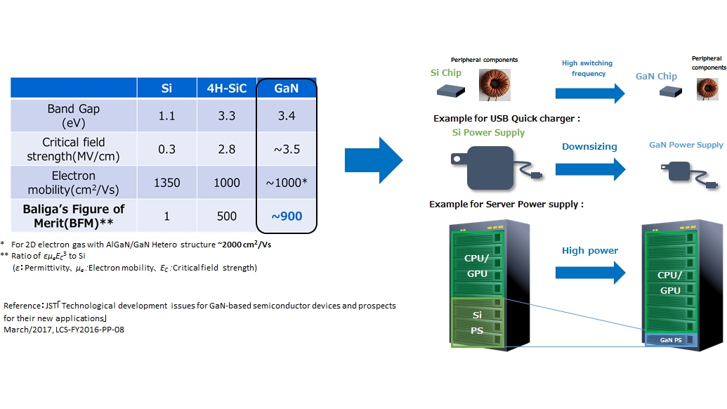
The energy conservation is attracting attention toward the realization of a carbon-free society, on the other hand, the demand for electric power continues to escalate. The need for highly efficient and compact electric power conversion systems increases rapidly. Not only improving the performance of Si power semiconductors, but also compound power semiconductors is introduced. We are expanding the product lineup of Si power semiconductors and increasing production capacity. In compound semiconductors, we commercialize SiC(Silicon carbide ) semiconductor products. Furthermore, we are advancing development for GaN (Gallium nitride) power devices.
By offering high-performance GaN power devices that are easier for customers to use, we will contribute to reduce power dissipation and reduction in size of customer's equipment.
Power device application scope
Si device is used current mainstream for power device. SiC device is expected for high power & efficiency application because of good heat conductivity. GaN device makes applications high efficiency & downsizing because of better switching characteristic.

GaN Power device advantages
GaN is a semiconductor material with high critical field strength and electron mobility. Therefore, when used in semiconductor devices, they achieve higher switching speed, and lower ON-resistance. GaN contributes to be lower power consumption, higher output, and reduction in size of customer's equipment because of high frequency switching and reducing the number of cooling units.
Toshiba GaN Power device
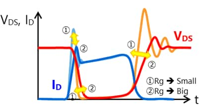
Easy Gate control
Because of Toshiba original Normally-ON + cascade structure,
Switching Slew Rate(dVDS/dt) are easy to control by series Gate Resistance(Rg).
(Conventional cascade type is difficult to control.)
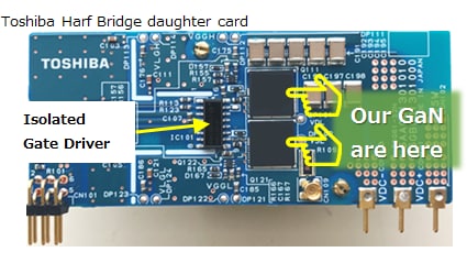
Configure high performance and ease of use
Propose Toshiba original peripheral circuit and appropriate board design
VDSS : 650V
RDS(ON) : 54mΩ (typ.)
Package : QFN9x9 (9mm×9mm)
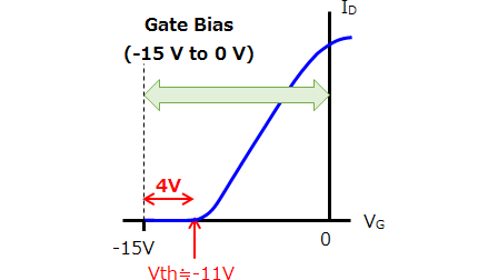
Improve Noise Immunity
Because of adopting original Normally-ON device,
it secures higher Vth, and is hard to cause malfunction
(In case of general Normally-OFF JFET, Vth is approximately 1.2V)
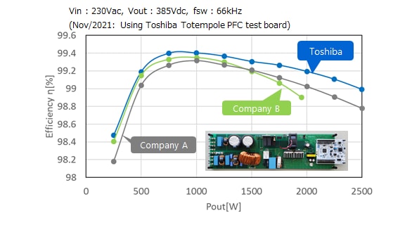
High efficiency
On our test sample with Totem-Pole PFC board, reached 99.4% peak efficiency(~2.5kW)
Confirmed higher efficiency than the others.
Related information
Click here for more research & development information of GaN power devices
Process Technology for MOS-Type GaN Devices Offering High Channel Mobility and High Reliability(348KB)
Toshiba Develops a Gate dielectric Process Technology for Improving the Reliability of GaN-MOSFET
Toshiba’s Cascode GaN Discrete Power Device Realize Stable Operation and Simplifies System Design with Direct Gate Drive
Click here for more information of other power devices
SiC Power Devices
MOSFET