
-
My ToshibaSemicon
- 반도체 탑
-
애플리케이션Automotive
Body Electronics
xEV
In-Vehicle Infotainment
Advanced Driver-Assistance Systems (ADAS)
Chassis
IndustrialInfrastructure
BEMS/HEMS
Factory Automation
Commercial Equipment
Consumer/PersonalIoT Equipment
Healthcare
Wearable Device
Mobile
Computer Peripherals
-
제품자동차 디바이스
Discrete Semiconductor
다이오드
트랜지스터
로직 IC
Analog Devices
Digital Devices
Wireless Devices
※
 : Products list (parametric search)파워반도체
※
: Products list (parametric search)Isolators/Solid State RelaysPhotocouplers
Digital Isolators
Solid State Relays
Fiber Optic Transmitting Modules
※
: Products list (parametric search)MOSFETsIGBTs/IEGTs바이폴라 트랜지스터※
: Products list (parametric search)다이오드※
: Products list (parametric search)마이크로컨트롤러모터 드라이버 ICIntelligent Power ICs※
: Products list (parametric search)전원관리IC리니어 IC※
: Products list (parametric search)범용로직IC리니어 이미지 센서기타 제품용 IC기타 제품용 IC
※
: Products list (parametric search) -
개발/설계 지원
-
기술 자료
- 구매처


- 부품 번호 & 키워드 검색
- 상호 참조 검색
- 파라미터 검색
- 재고 확인 및 구매
This webpage doesn't work with Internet Explorer. Please use the latest version of Google Chrome, Microsoft Edge, Mozilla Firefox or Safari.
3글자 이상 입력하세요. Search for multiple part numbers fromhere.
The information presented in this cross reference is based on TOSHIBA's selection criteria and should be treated as a suggestion only. Please carefully review the latest versions of all relevant information on the TOSHIBA products, including without limitation data sheets and validate all operating parameters of the TOSHIBA products to ensure that the suggested TOSHIBA products are truly compatible with your design and application.Please note that this cross reference is based on TOSHIBA's estimate of compatibility with other manufacturers' products, based on other manufacturers' published data, at the time the data was collected.TOSHIBA is not responsible for any incorrect or incomplete information. Information is subject to change at any time without notice.
3글자 이상 입력하세요.
Contributes to high efficiency and low loss of high output power supply
SiC (silicon carbide) is a compound semiconductor material composed of silicon (Si) and carbon (C). Compared to Si, this material has a wider bandgap and therefore has a higher dielectric breakdown field strength and better thermal conduction. The Schottky Barrier Diode (SBD) made of SiC features high reverse voltage. Our products employ an improved JBS (Junction Barrier controlled Schottky) structure to achieve low leakage current (reverse current) and high surge current (non-repetitive peak forward surge current) required for switching power supply applications in addition to the high-speed reverse recovery characteristics, which are features of SBD.
Our latest second-generation products have reduced (VF・Qcj※1) ※2 by about 67% compared to the first-generation products, which is a critical figure of merit for switching applications such as power supplies.
In order to cope with the increasing power capabilty of equipment, we have added two products with a forward DC current of 12A, "TRS12A65F" with an isolation-type package TO-220F-2L, and "TRS12E65F" with a non-isolation-type package TO-220-2L to our lineup. These products achieve a high non-repetitive peak forward current of 97 A (max) (for TRS12E65F) and a low forward voltage of 1.45 V (typ.), contributing to power savings and higher efficiency in equipment.
※ 1 Qcj: Total capacitive charge of the junction capacitance with a reverse voltage of 0.1 V to 400 V
※ 2: An index for comparing the suitability for switching applications by calculating the product of the forward voltage and charge quantity characteristics in a trade-off relationship. The smaller this value, the better the performance.
Features
- Large non-repetitive peak forward surge current: IFSM = 97 A (TRS12E65F)
- Low reverse current: IR = 0.3 to 0.6 μA (typ.)
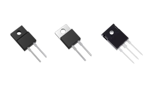
- Line-up of three types of packages: isolation type TO-220F-2L, non-isolation type TO-220-2L, non-isolation type TO-247
- Useful application notes, reference designs, and other documents on the web.
Improved JBS Structure Achieving Low Leakage Current and High Surge Current Capability
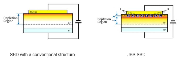
SBDs generally have the advantages of very sort reverse recovery time and low forward voltage, but they also have the disadvantages of high leakage current (reverse current) and low surge current capability (non-repetitive peak forward surge current). We have improved this disadvantage by adopting an improved JBS structure.
SBDs combine semiconductors and metals to realize diodes because of their work function differences. At this junction surface, the molecular structure may be discontinuous, surface irregularities, crystal defects, etc. When a high electric field is applied across a semiconductor-metal interface with many such defects, a current called leakage current flows.
In SBDs with conventional structure, the depletion region extends into the semiconductor side as shown in Figure 1, causing the electric field produced by electric charge (or electron) to be the strongest at the semiconductor-metal interface.
In contrast, in a JBS diode, the depletion region extends between p and n- regions that are partially buried below the semiconductor surface. When the reverse bias voltage increases, p-type depletion regions punch through each other and the position of the maximum electric field moves directly under the p region. This reduces the electric field on the surface that has a high probability of defects, thereby reducing leakage current.
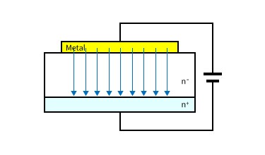
When a conventional SBD is forward-biased, current flows through the following path as shown in Figure 2:
metal -> Schottky barrier -> n- layer -> n+ layer. At this time, the n- layer has relatively large resistive components because of low dopant concentration. Therefore, the effect of heat generation due to the resistance component is large and the capability to allow large current in the forward direction, such as surge current, is limited.
In order to realize high surge current capability, we have developed improved JBS-structure products incorporating the concepts of MPS (Merged PiN Schottky) structure.
The MPS structure has p+ regions buried in the n- region of an SBD. (In our design, part of the p-layer of the JBS structure is enlarged and the impurity concentration of this part is increased.) The p+ regions and the n- region of original SBD form a pn junction diode, which turns on when large current (high surge current) is needed. This increases the current-carrying capability of the SBD and reduces a rise in forward voltage even at high current then high surge current capability is acheived.
For details on the improved JBS structure, please refer to the following.
Product Specifications
Part number |
|||||||
|---|---|---|---|---|---|---|---|
| Data sheet | |||||||
Package |
TO-220F-2L |
TO-220-2L
|
TO-247
|
||||
Absolute maximum ratings |
Repetitive peak reverse Voltage VRRM (V) |
650 |
|||||
Forward DC current IF(DC) (A) |
12 |
24 |
20 |
16 |
12 |
||
Non-repetitive peak forward surge current IFSM (A) @t=10 ms |
92 |
97 |
92 |
79 |
65 |
52 |
|
Junction temperature Tj (°C) |
175 |
||||||
Electrical characteristics |
Reverse current IR typ. (μA) @VR=650 V |
0.6 |
0.6 |
0.5 |
0.4 |
0.3 |
|
Forward voltage VF typ. (V) |
1.45 @IF=12 A |
1.45 @IF=12 A |
1.45 @IF=10 A |
1.45 @IF=8 A |
1.45 @IF=6 A |
||
Total capacitive charge Qcj typ. (nC) @VR=0.1~400 V |
30 |
30 |
24 |
19.4 |
15 |
||
Thermal characteristics |
Thermal resistance (junction/case) Rth(j-C) max (°C/W) |
3.65 |
1.3 |
1.3 |
1.4 |
1.8 |
2.2 |


