- General Top
- SEMICONDUCTOR
- STORAGE
- COMPANY
-
My ToshibaSemicon
- Semiconductor Top
-
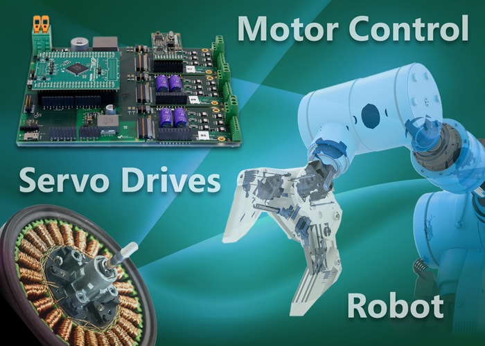
ApplicationsAutomotive
Body Electronics
xEV
In-Vehicle Infotainment
Advanced Driver-Assistance Systems (ADAS)
Chassis
IndustrialInfrastructure
BEMS/HEMS
Factory Automation
Commercial Equipment
Consumer/PersonalIoT Equipment
Healthcare
Wearable Device
Mobile
Computer Peripherals
-
ProductsAutomotive Devices
Discrete Semiconductor
Diodes
Transistors
Logic ICs
Analog Devices
- Automotive SmartMCD™ (Integreted SoC Conbining Microcontroller and Driver)
- Automotive Brushless Motor Driver ICs
- Automotive Brushed DC Motor Driver ICs
- Automotive Stepping Motor Driver ICs
- Automotive Driver ICs
- Automotive System Power Supplies ICs
- Automotive audio power amplifier ICs
- Automotive Network Communication
Digital Devices
Wireless Devices
※
 : Products list (parametric search)Power Semiconductors
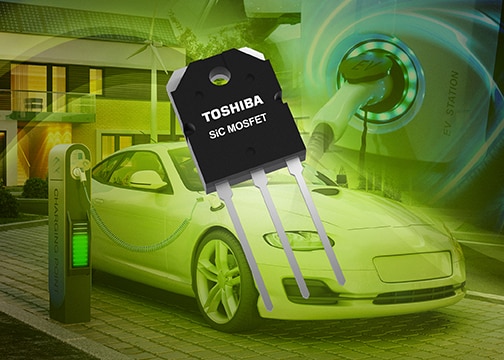
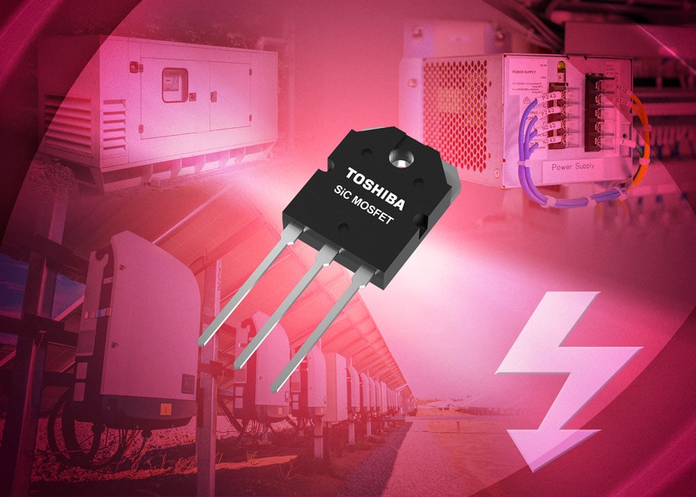
SiC Power Devices
※
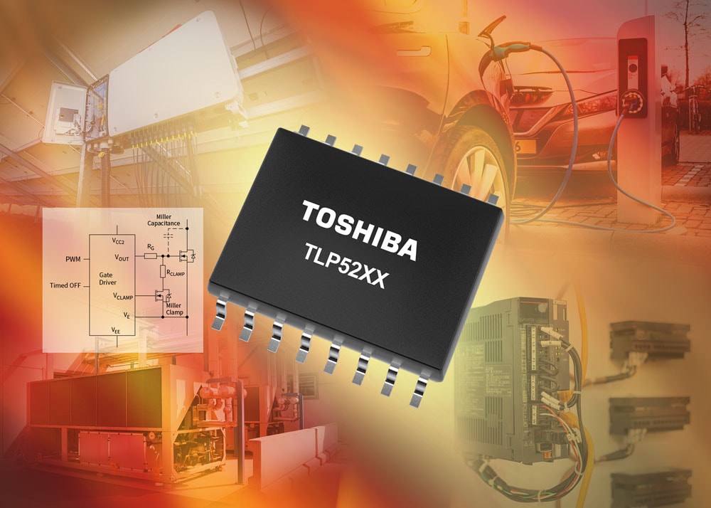
: Products list (parametric search)Isolators/Solid State RelaysPhotocouplers
Digital Isolators
Solid State Relays
Fiber Optic Transmitting Modules
※
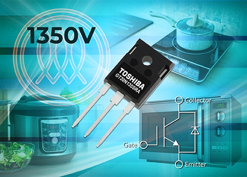
: Products list (parametric search)MOSFETsIGBTs/IEGTsBipolar Transistors※
: Products list (parametric search)Diodes※
: Products list (parametric search)MicrocontrollersMotor Driver ICsIntelligent Power ICs※
: Products list (parametric search)Power Management ICsLinear ICs※
: Products list (parametric search)General Purpose Logic ICsLinear Image SensorsOther Product ICsOther Product ICs
※
: Products list (parametric search) -
Design & Development
Design & Development
Innovation Centre
At the Toshiba Innovation Centre we constantly strive to inspire you with our technologies and solutions. Discover how to place us at the heart of your innovations.
-
Knowledge
Knowledge
Highlighted Topics
Further Materials
Other
- Where To Buy


- Part Number & Keyword Search
- Cross Reference Search
- Parametric Search
- Stock Check & Purchase
This webpage doesn't work with Internet Explorer. Please use the latest version of Google Chrome, Microsoft Edge, Mozilla Firefox or Safari.
require 3 characters or more. Search for multiple part numbers fromhere.
The information presented in this cross reference is based on TOSHIBA's selection criteria and should be treated as a suggestion only. Please carefully review the latest versions of all relevant information on the TOSHIBA products, including without limitation data sheets and validate all operating parameters of the TOSHIBA products to ensure that the suggested TOSHIBA products are truly compatible with your design and application.Please note that this cross reference is based on TOSHIBA's estimate of compatibility with other manufacturers' products, based on other manufacturers' published data, at the time the data was collected.TOSHIBA is not responsible for any incorrect or incomplete information. Information is subject to change at any time without notice.
require 3 characters or more.
Isolating I2C designs with optocouplers
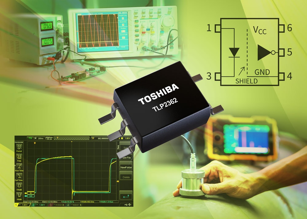
I2C was only designed and intended for low-latency board-level communication, meaning that latencies between isolated circuits must be carefully considered.
One concern is the ACK/NACK response of the target to the controller, which According must be valid after a setup time of 0.45µs in fast mode plus operation (1MHz). Additionally, there is timing for data setup - in fast mode a target is expected to set up the SDA signal within 50ns after the falling edge of the previous clock bit.
In both cases, latency through an isolation circuit could cause problems in fulfilling the timing specified in the standard. As a result, the circuit design should keep the latency as low as possible to ensure reliable operation, especially at the fastest SCL speeds.
Selecting an optocoupler for an I2C isolator is not trivial. The input / output propagation delay must be short enough to allow normal bus operation and the device must support the controller voltage. Additionally, the optoisolator needs to have an open-drain output as open Drain or open Collector is standard with the I²C bus. Alongside these criteria, designers also need to consider board real estate, component count, and cost.
A fully multi master compatible I2C optoisolator circuit requires four optocoupler devices, two for SDA and two for SCL. To save cost and board space, this can be reduced to three optocouplers in single master environment.
Toshiba’s TLP2362 optoisolator uses a high-output infrared LED coupled with a high-gain, high-speed photodetector. Operating from supply voltage of 2.7V to 5.5V enables it to directly interface to 3.3V and 5V I/Os. Reinforced insulation requirements up to 3750 V can be met. Its operating temperature extends from -40°C to 125°C while its internal Faraday cage protects against common-mode transient signals of minimum ±20kV/µs, ensuring robust I2C communication even in noisy, industrial applications that can be very challenging. Furthermore, this optocoupler is UL and cUL recognised and VDE and CQE approved.
The device is housed in an SO6 package (3.7 × 7mm) with five pins. Only a single ceramic 1 µF bypass capacitor is required to be placed near the device to stabilise the operation of the output logic, ensuring that the photocoupler switches correctly. Propagation time delay is just 35ns (max. 100ns) for high-to-low signal transitions and 26ns (max. 100ns) for low-to-high transitions. The device-to-device skew is only ±40ns, ensuring good consistency between manufactured boards.
Toshiba has published a white paper on using optocouplers to isolate the I2C bus – to download your free copy, please click here: