Power semiconductors. Essential devices for a carbon-neutral future.

By bringing the latest technology advances to high performance power semiconductors, Toshiba Electronic Devices and Storage Corporation is boosting energy conservation in all types of electrical equipment and contributing to a carbon-neutral world.

What they do

Switch on a PC and get down to work. While it adds to your productivity, the PC is also dissipating power—and the same is true for every other electronic device, large and small. Power semiconductors step in to micromanage electricity flows and cut power loss. They deliver energy savings in everything from PCs and smartphones to cars, trains and electricity substations. They may be small, but our high performance power semiconductors make a huge difference.

Our power semiconductors

Customers worldwide rely on our power semiconductor to bring new levels of operating efficiency to their products.

Decarbonized future

Even as the drive for decarbonization intensifies, demand for electricity continues to grow. The need for smaller power converters with low power loss has never been greater, and we are responding by improving the performance of our silicon (Si) devices and introducing wide-bandgap (WBG) semiconductors. We are expanding our Si products lineup and building new manufacturing facilities to boost their production. In our WBG lineup, we have commercialized silicon carbide (SiC) devices and we are developing gallium nitride (GaN) power semiconductors.
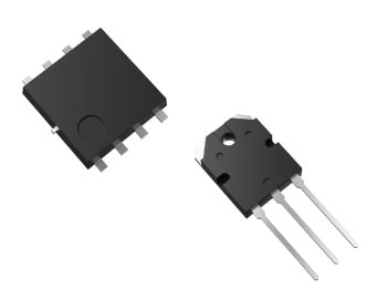
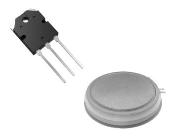
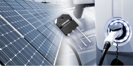
SiC power devices
SiC surpasses Si in its high electric breakdown field, saturated electron velocity, and thermal conductivity. It brings higher voltage resistance, higher-speed switching, and lower on-resistance to semiconductors, and is widely seen as a next-generation low-loss device that will advance lower power consumption and system downsizing.
Toshiba GaN power device balances performance and ease of use
Another route to highly efficient, compact power conversion systems is GaN, but it brings its own challenges. Our gate dielectric process technology advances device reliability, and greatly reduces variation in characteristics such as threshold voltage. GaN MOSFETs using this technology will win GaN's further adoption.
MOSFETs
MOSFETs
Our extensive portfolio of low-VDSS and mid/high-VDSS MOSFETs offers various circuit configurations and packages. Their characteristics include high speed, high performance, low loss, low on-resistance and small packages.
IGBTs/IEGTs
IGBTs/IEGTs[Note 1]
Insulated gate bipolar transistors, IGBT, and injection enhanced gate transistors, IEGT, operate like MOSFETs and control the voltage between a gate and emitter, switching power on and off between a collector and emitter.
Diodes
Diodes[Note 2]
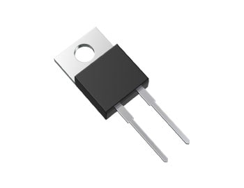
Our extensive portfolio includes high-speed, low-loss Schottky-barrier diodes (SBDs) and TVS diodes (ESD protection diodes) for high-speed signal lines.

[Note 1] IEGTs: Injection Enhanced Gate Transistor
[Note 2] Diodes: includes products other than power semiconductors

e-Learning

You can see the video from “What is Semiconductor?” to the “Fundamental of Power Semiconductors”. 

Reference Design
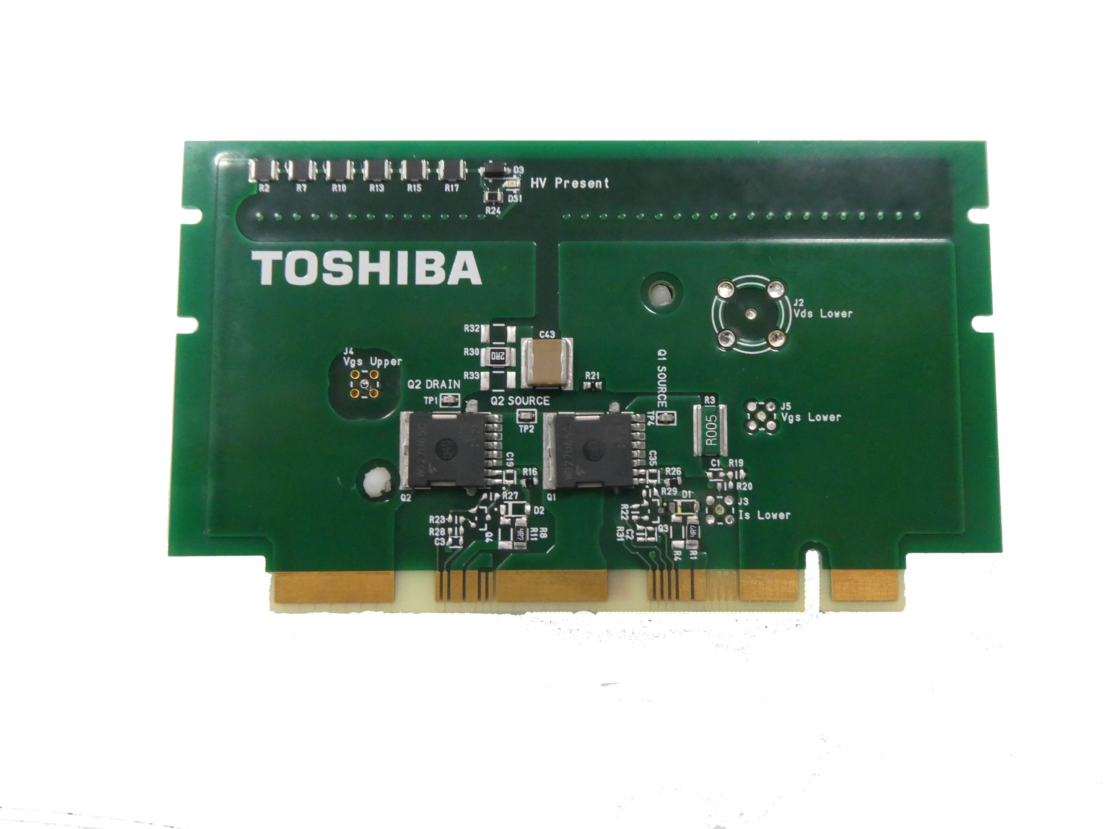
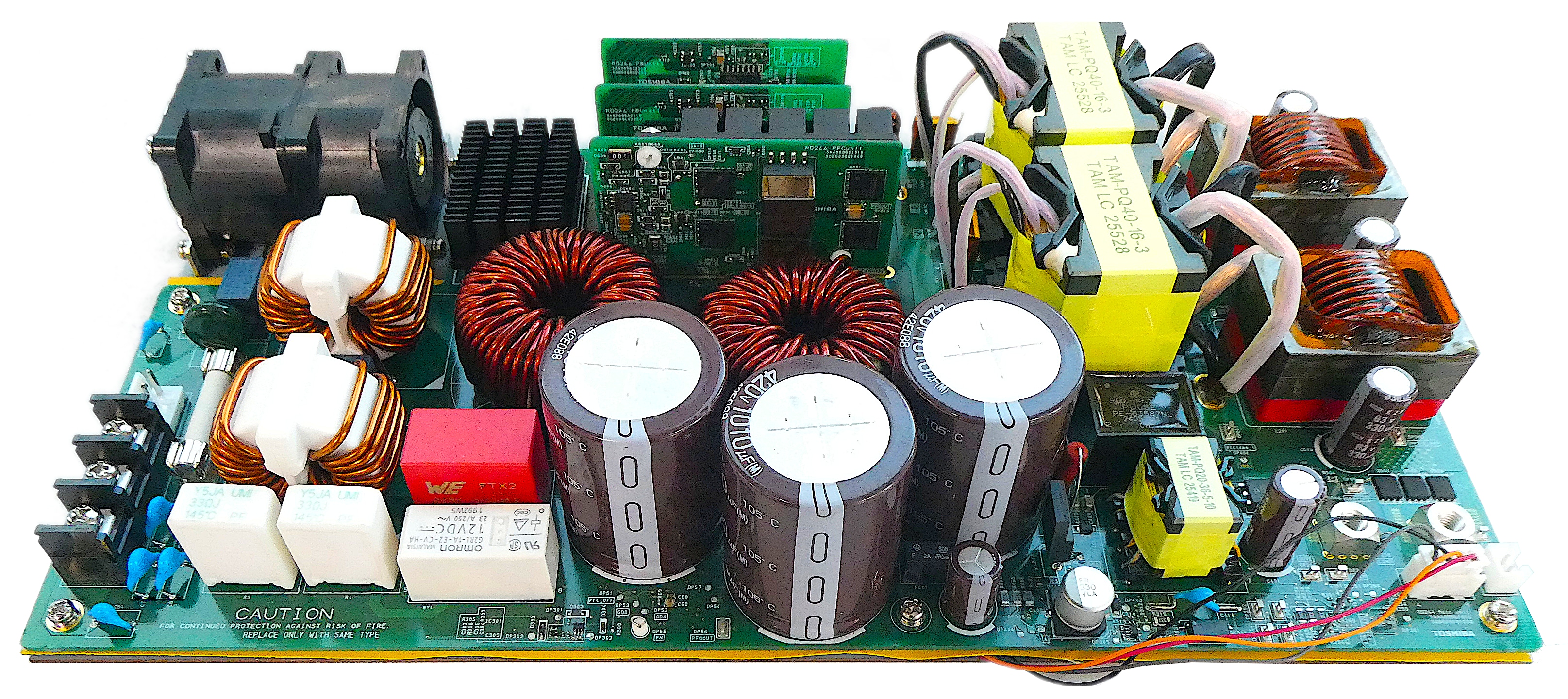
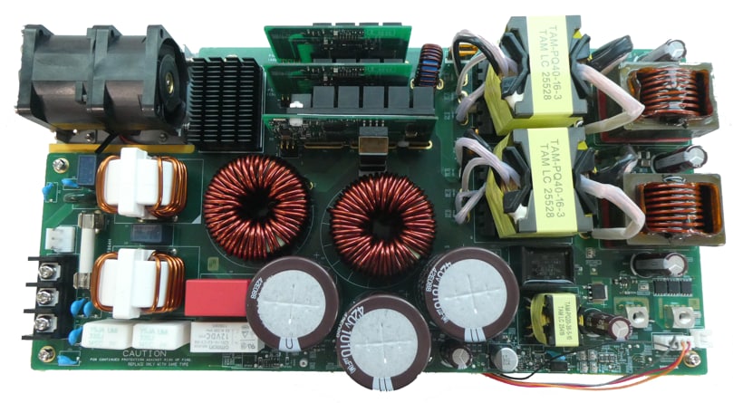
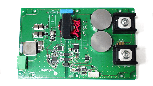
PCB Photo (example)
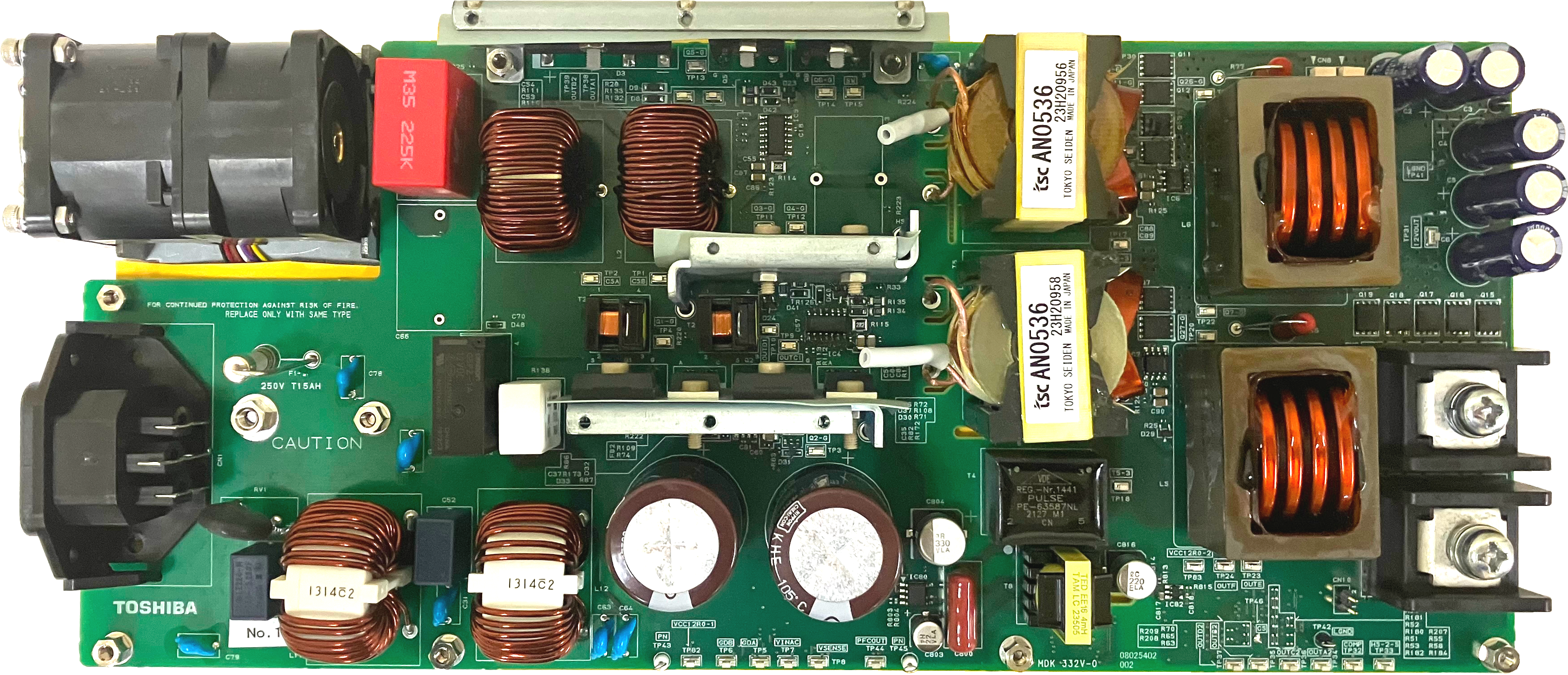
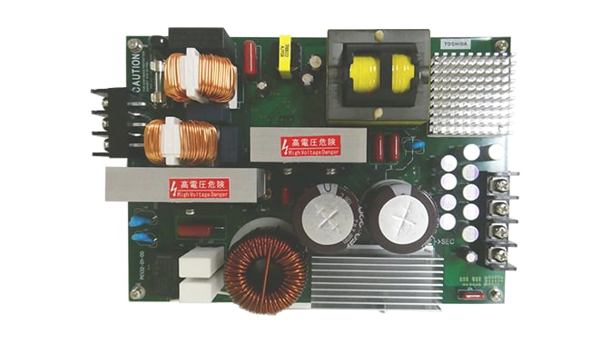
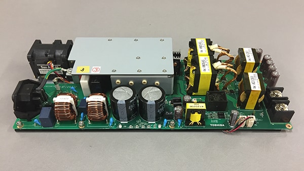
1.6 kW Server Power Supply (Upgraded)
Thanks to Toshiba’s latest power devices and digital isolator, this 1U size and 12 V output 1.6 kW server power supply achieves higher efficiency at whole load than the existing reference design which uses the same circuit topology. Design files and guides for circuit design and operation are available as reference design.
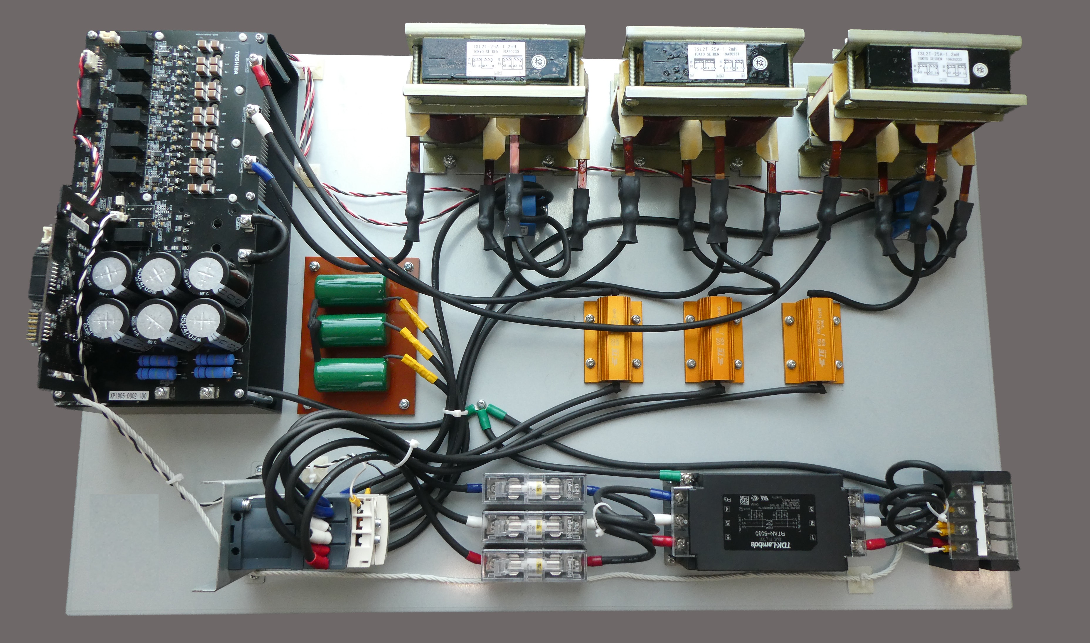
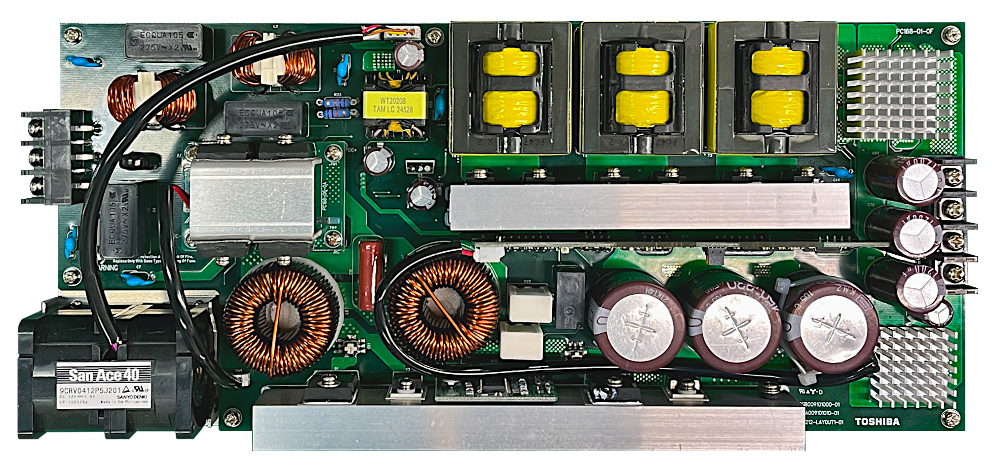
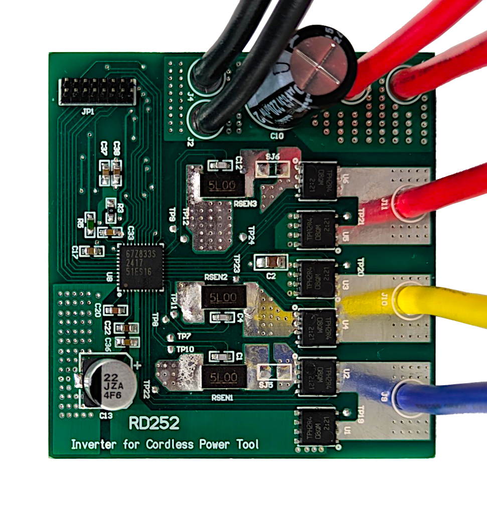
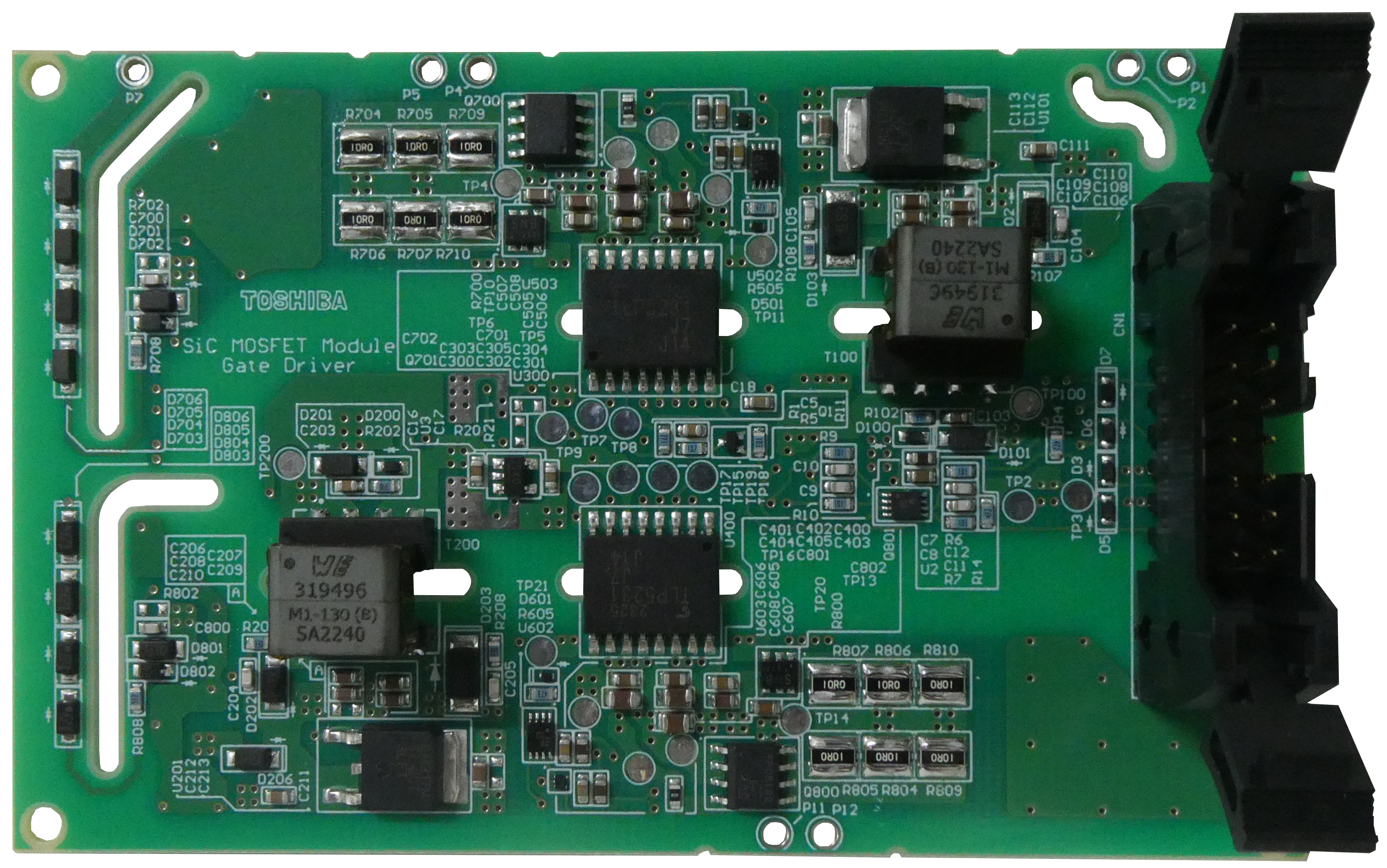
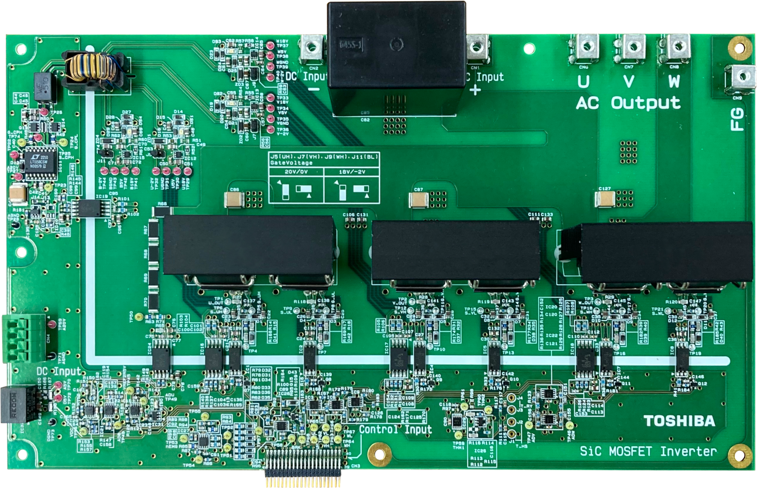
3-Phase Inverter Using SiC MOSFET
This reference design provides design guide, data and other contents of the 3-phase inverter using 1200 V SiC MOSFET. It drives AC 440V motors.
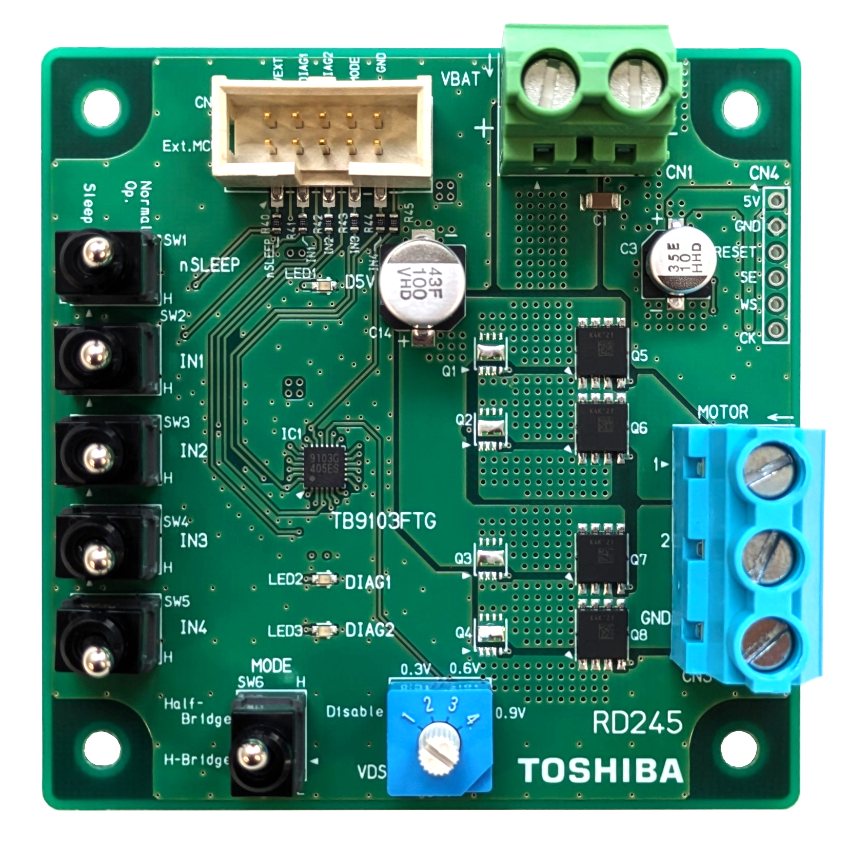
Automotive Brushed DC Motor Control Circuit Using TB9103FTG
The Automotive Brushed DC Motor Control Circuit Using TB9103FTG can control two motors in half-bridge mode or one motor in H-bridge mode. The Motor can be controlled using onboard switches or an external MCU. This reference design provides design guide, data, and other contents.
PCB Photo (example)
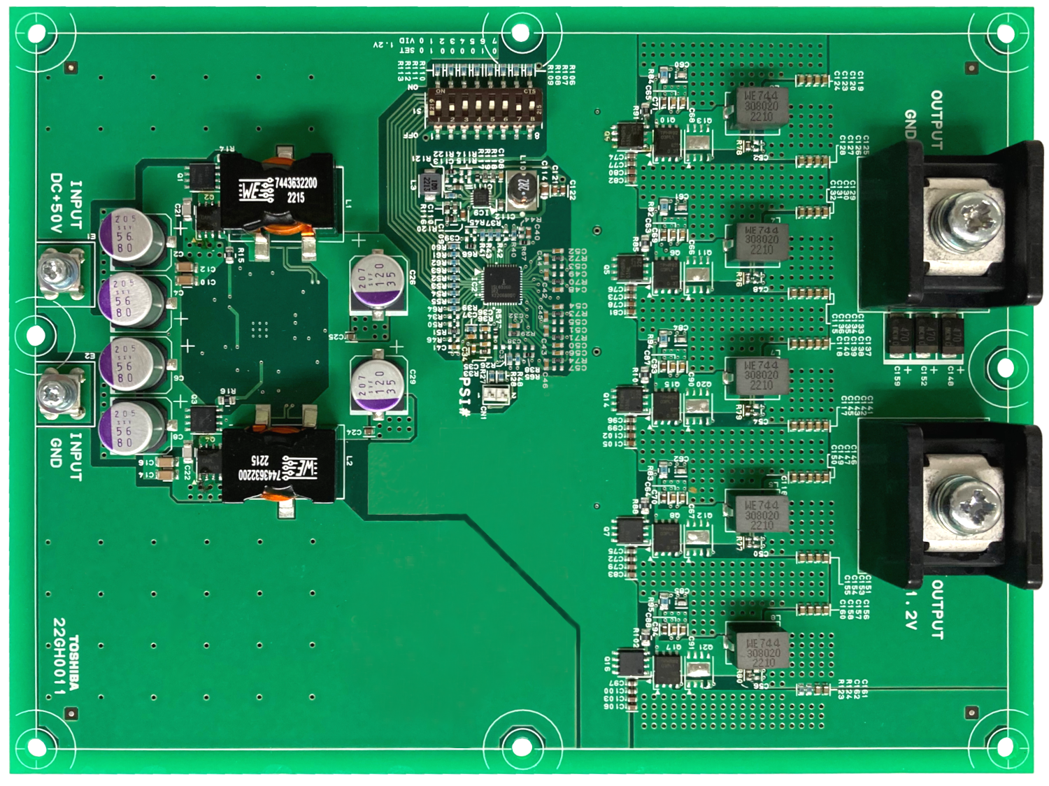
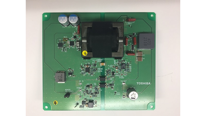
48 V Bus Compatible 1.2 V/100 A Double Step-Down DC-DC Converter
In recent years, saving energy in servers has become an urgent issue because of the rapid increase in server power consumption. To resolve the issue, Toshiba has developed this 48V bus compatible DC-DC converter with 1.2V/100A output.This design is a two-stage DC-DC converter capable of delivering 1.2V/100A to various devices from the 48V bus line. Since each stage uses Toshiba power MOSFETs that have good balance between on-resistance and charge characteristics, it achieves high efficiency. Design tips on each portion of the circuit, method of operation, and design information such as circuit diagrams and PCB patterns are available, please use them for your design.
PCB Photo (example)
1.6 kW Server Power Supply (Upgraded)
Thanks to Toshiba’s latest power devices and digital isolator, this 1U size and 12 V output 1.6 kW server power supply achieves higher efficiency at whole load than the existing reference design which uses the same circuit topology. Design files and guides for circuit design and operation are available as reference design.
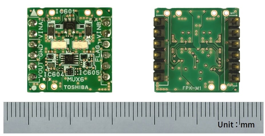
PCB photo example of Power multiplexer circuit
Power Multiplexer Circuit Using Common-Drain MOSFET
This power multiplexer circuit with 2 inputs and 1 output is realized on a small board. A new power multiplexer circuit usign common-drain MOSFET has been added to the already developed power multiplexer circuit reference design. These reference circuits allow switching between BBM and MBB modes by combining optimal devices such as MOSFET gate driver ICs and zener diodes from our diverse product lineup.
Power multiplexer circuit / 2 input and 1 output
3-Phase Inverter Using SiC MOSFET
This reference design provides design guide, data and other contents of the 3-phase inverter using 1200 V SiC MOSFET. It drives AC 440V motors.
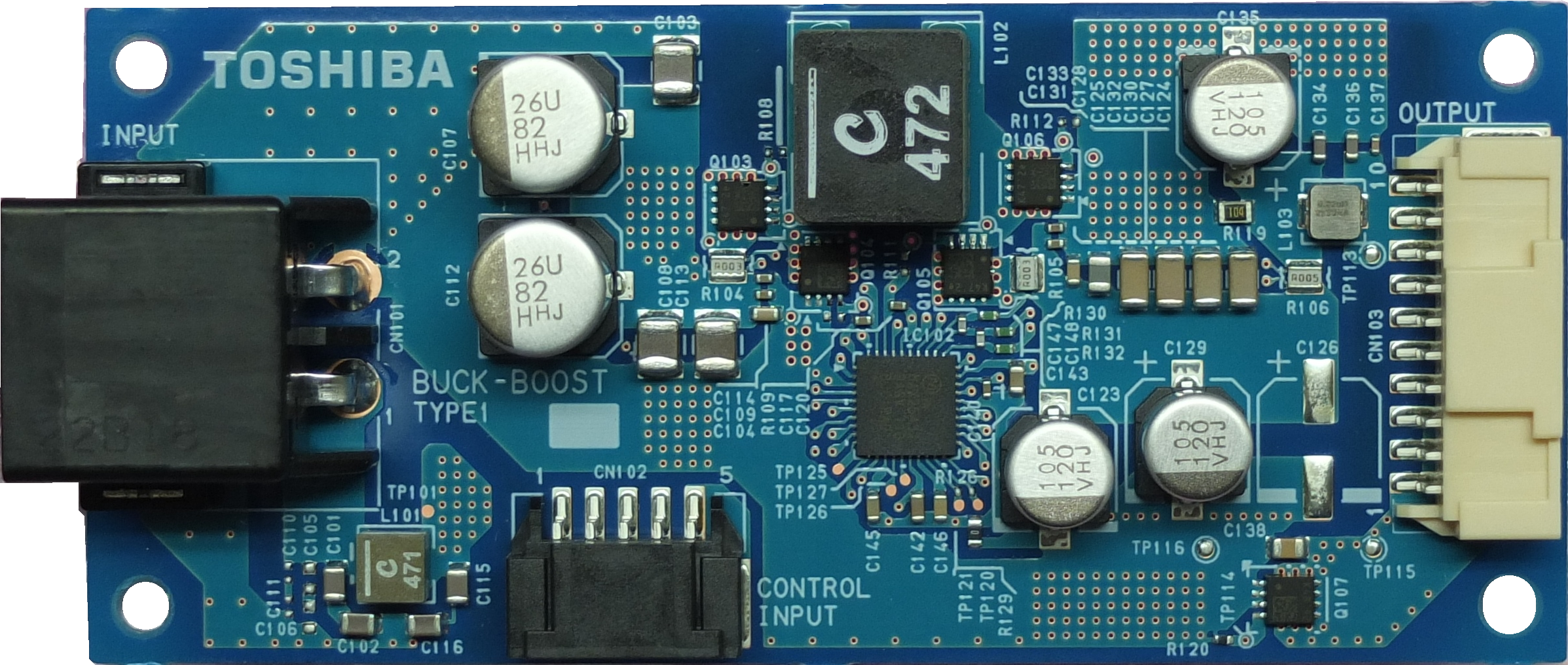
Automotive Buck-Boost DC-DC Converter for USB PD
This reference design provides design guide, data and other contents of Automotive Buck-Boost DC-DC Converter for USB PD.
PCB Photo (example)
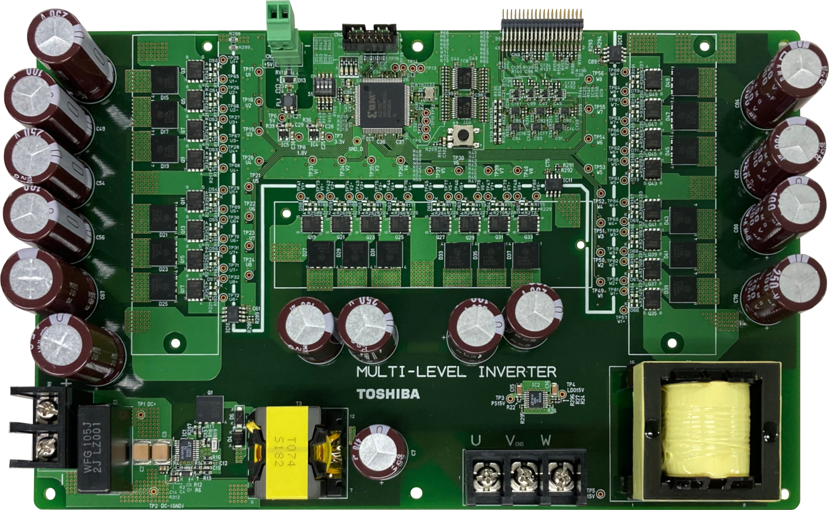
3-Phase Multi-Level Inverter using MOSFET
This reference design provides design guide, data and other contents of the 3-Phase Multi-Level Inverter with 5 level output. It uses 150 V MOSFETs to drive AC 200 V Motor.
PCB Photo (example)
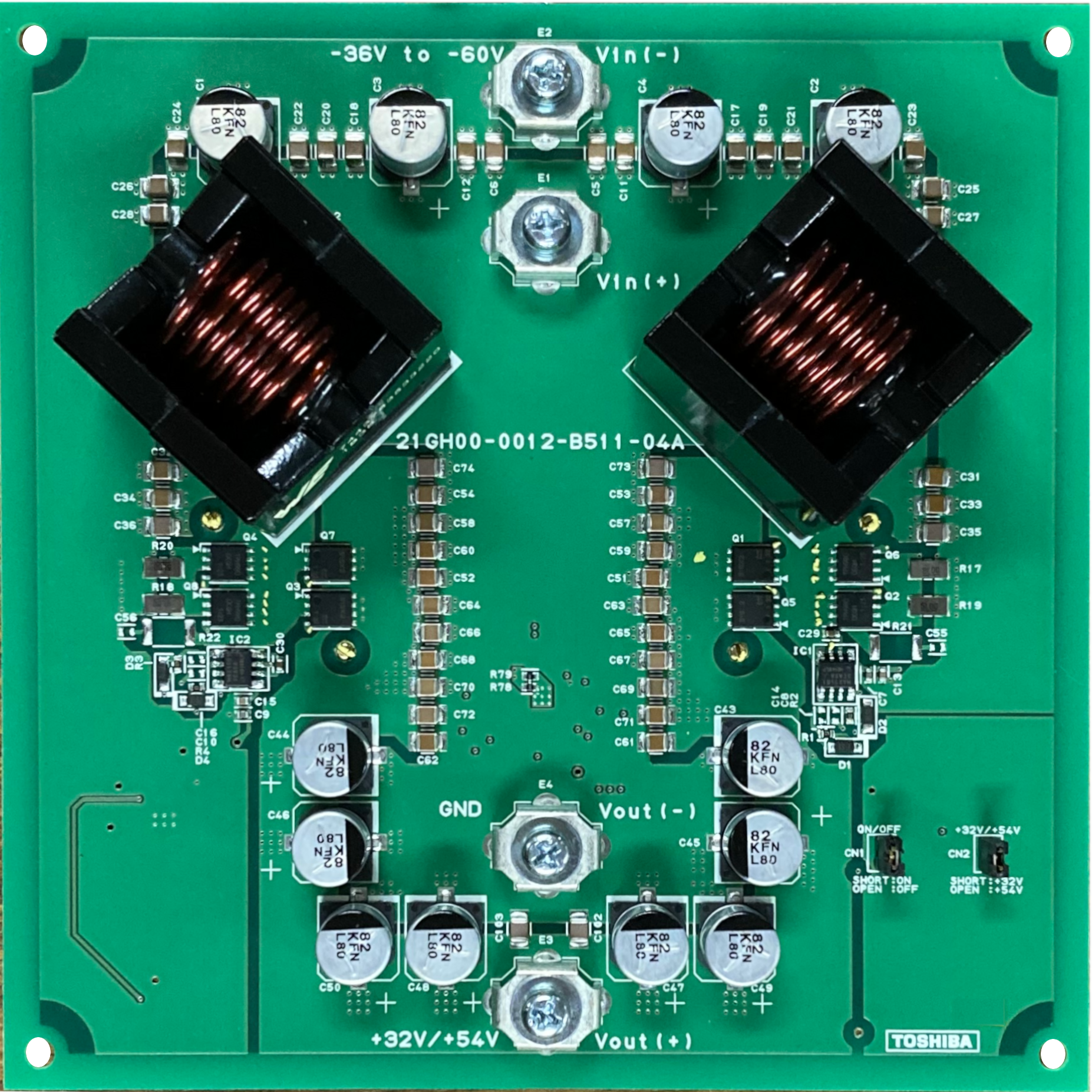
1 kW Non-Isolated Buck-Boost DC-DC Converter for Telecommunication Equipment
This reference design provides design guide, data and other contents of 1 kW Non-Isolated Buck-Boost DC-DC Converter for Telecommunication Equipment.
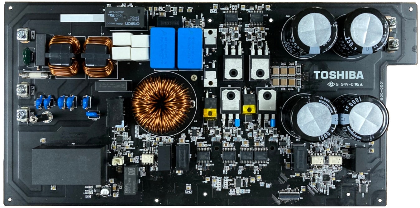
1.6 kW T-Type 3-Level PFC Power Supply
This reference design provides design guide, data and other contents of 1.6kW AC-DC converter power supply using T-Type 3-Level power factor correction (PFC) circuit.
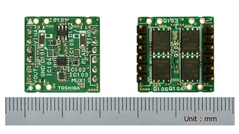
PCB photo example of Power multiplexer circuit
Power multiplexer circuit
In this reference design, a Power multiplexer circuit with 2 input and 1 output is implemented on a small PCB. MOSFET gate driver ICs, eFuse ICs, zener diodes and small package MOSFETs selected from Toshiba's diverse lineup are used create ideal diode like characteristics with BBM and MBB switching.
Power multiplexer circuit / 2 input and 1 output
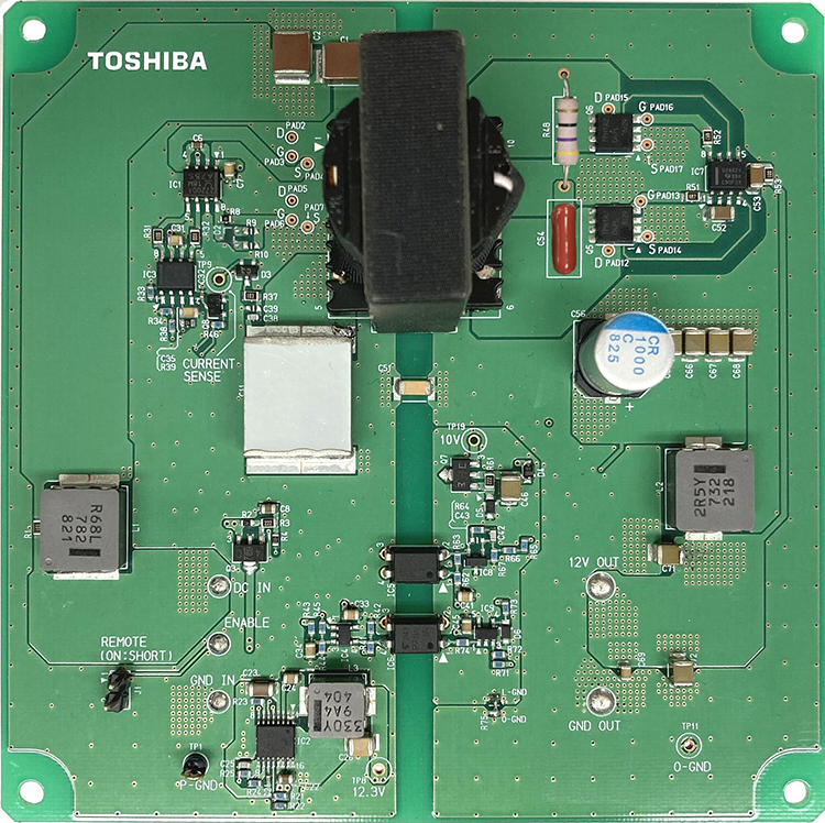
Board photo of 100 W LLC DC-DC Converter
100 W LLC DC-DC Converter
This reference design provides design guide, data and other contents of 100 W LLC DC-DC Converter which uses Zero Volt Switching implemented using LLC resonance.
DC-DC Converter / MOSFET / Isolators
Exterior photo of 200 W active clamp forward DC-DC converter.
200 W Active Clamp Forward DC-DC Converter
This reference design provides design guide, data and other contents of 1 kW server power supply using phase shifetd full-bridge DC-DC converter.
DC-DC Converter
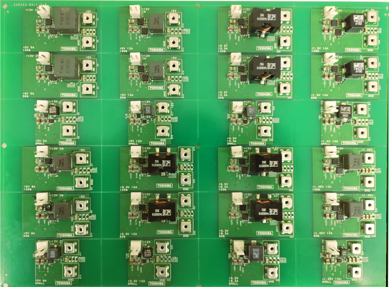
Photo of non-isolated buck DC-DC converter.
Non-Isolated Buck DC-DC Converter
This reference design provides design guide, data and other contents of multiple non-isolated buck DC-DC converter power supplies. Multiple variations of the power supply are optimized for various outputs, loads and board mounting areas.
Reference Design Center
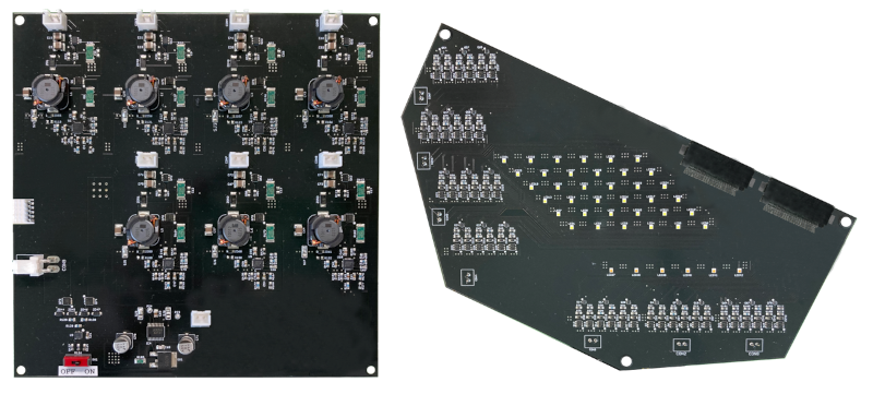
Photo of Matrix LED Headlight
Matrix LED Headlight
This reference design provides design guide, data and other contents of LED Matrix Headlight. It controls the lighting of multiple LEDs independently according to the situation.
Reference Design Center
Features of 500 W server power supply using TOLL package DTMOS.
500 W Server Power Supply using TOLL Package DTMOS
This reference design provides design guide, data and other contents of 500 W server power supply using continuous current mode PFC and LLC DC-DC converter. Using TOLL package MOSFET in the PFC circuit, decreases the overall size and increases the power density.
500 W Server / TOLL Package / DTMOS
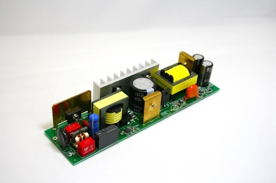
Photo of 100 W power supply for LED Lighting.
100 W Power Supply for LED Lighting
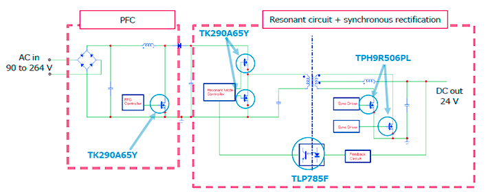
This reference design provides design guide, data and other contents of the constant current 100 W Power Supply for LED Lighting with PFC and a wide range of input voltage i.e. AC90V to 264V.
Reference Design Center
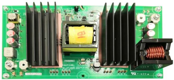
Exterior photo of 1 kW full-bridge DC-DC converter.
1 kW Full-Bridge DC-DC Converter
This reference design provides design guide, data and other contents of 1 kW server power supply using phase shifetd full-bridge DC-DC converter.
Full-Bridge / DC-DC Converter
Exterior photo of 1.6 kW 48 V output telecommunication equipment power supply.
1.6 kW 48 V Output Telecommunication Equipment Power Supply
This reference design provides design guide, data and other contents of 1.6 kW 48 V output power supply using semi-bridgeless PFC and isolated phase-shift full-bridge DC-DC converter.
Power Supply
Circuit of active clamp forward DC-DC power supply basic simulation circuit.
Active Clamp Forward DC-DC Power Supply Basic Simulation Circuit
This reference design provides OrCAD® based simulation circuit, simulation results and design guide. This is for designing Active Clamp Forward topology of DC-DC power supply.
Simulation Circuit / Editable on OrCAD®
Circuit of active clamp forward AC-DC power supply basic simulation circuit.
Active Clamp Forward AC-DC Power Supply Basic Simulation Circuit
This reference design provides OrCAD® based simulation circuit, simulation results and design guide. This is for designing Active Clamp Forward topology of AC-DC power supply.
Simulation Circuit / Editable on OrCAD®
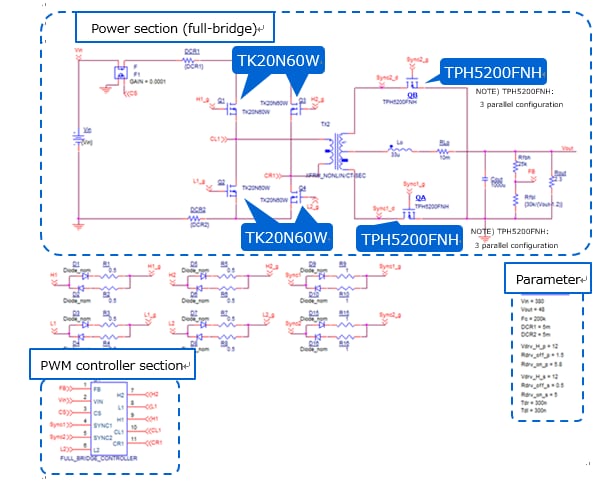
Circuit of Full-Bridge DC-DC power supply basic simulation circuit.
Full-Bridge DC-DC Power Supply Basic Simulation Circuit
This reference design provides OrCAD® based simulation circuit, simulation results and design guide. This is for designing Full-Bridge topology of DC-DC power supply.
Simulation Circuit / Editable on OrCAD®
Circuit of Full-Bridge AC-DC power supply basic simulation circuit.
Full-Bridge AC-DC Power Supply Basic Simulation Circuit
This reference design provides OrCAD® based simulation circuit, simulation results and design guide. This is for designing Full-Bridge topology of AC-DC power supply.
Simulation Circuit / Editable on OrCAD®
Circuit of Non-isolated Synchronous Buck DC-DC power supply basic simulation circuit.
Non-isolated Synchronous Buck DC-DC Power Supply Basic Simulation Circuit
This reference design provides OrCAD® based simulation circuit, simulation results and design guide. This is for designing Non-isolated Synchronous Buck DC-DC power supply.
Non-isolated / Synchronous / Buck / DC-DC / Power Supply
Circuit of Half-Bridge (HB) AC-DC power supply basic simulation circuit.
Half-Bridge (HB) AC-DC Power Supply Basic Simulation Circuit
This reference design provides OrCAD® based simulation circuit, simulation results and design guide. This is for designing Half-Bridge (HB) topology of AC-DC power supply.
Half-Bridge / AC-DC / Power / Supply
Circuit of Half-Bridge (HB) DC-DC power supply basic simulation circuit.
Half-Bridge (HB) DC-DC Power Supply Basic Simulation Circuit
This reference design provides OrCAD® based simulation circuit, simulation results and design guide. This is for designing Half-Bridge (HB) topology of DC-DC power supply.
Half-Bridge / DC-DC / Power / Supply
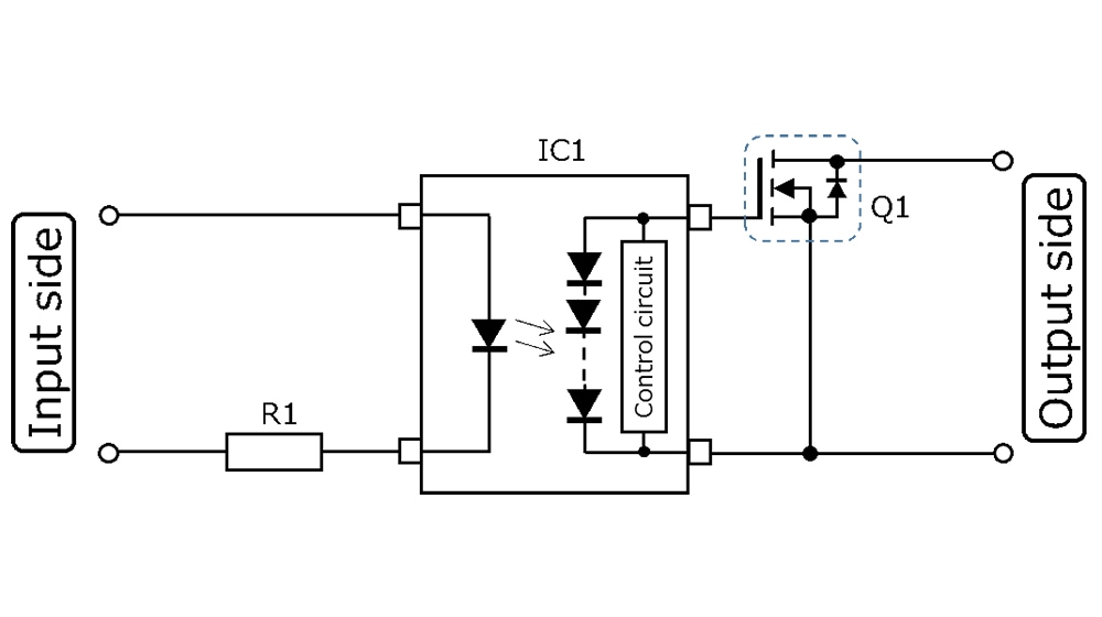
HVAC application of photovoltaic-output photocoupler and MOSFET as replacement for mechanical relay.
Photovoltaic-Output Photocoupler and MOSFET as Replacement for Mechanical Relay
Solid state relay with photovoltaic-output coupler, TLP3906, and MOSFET, TPH1R306PL. Describes design guidance of solid state relay circuit as replacement of mechanical relay.
Photovoltaic / Output / Photocoupler / MOSFET / Replacement / Mechanical Relay
Features of 1.2V/100A output DC-DC converter compliant with 48V bus voltage.
1.2V/100A Output DC-DC Converter Compliant with 48V Bus Voltage
This reference design provides specification, block diagram and PCB layout data of 1.2V/100A output isolated DC-DC converter which convert 48V bus voltage to 1.2V directly.
DC-DC / MOSFET / reference design
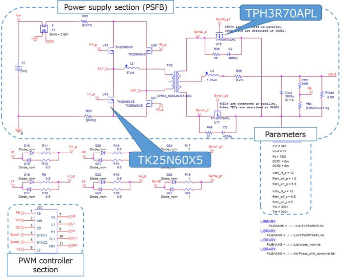
Circuit of phase-shift full bridge (PSFB) AC-DC power supply basic simulation circuit.
Phase-Shift Full Bridge (PSFB) AC-DC Power Supply Basic Simulation Circuit
This reference design provides OrCAD® based simulation circuit, simulation results and design guide. This is for designing phase-shift full bridge (PSFB) topology of AC-DC power supply.
PSFB / AC-DC / MOSFET / Reference design
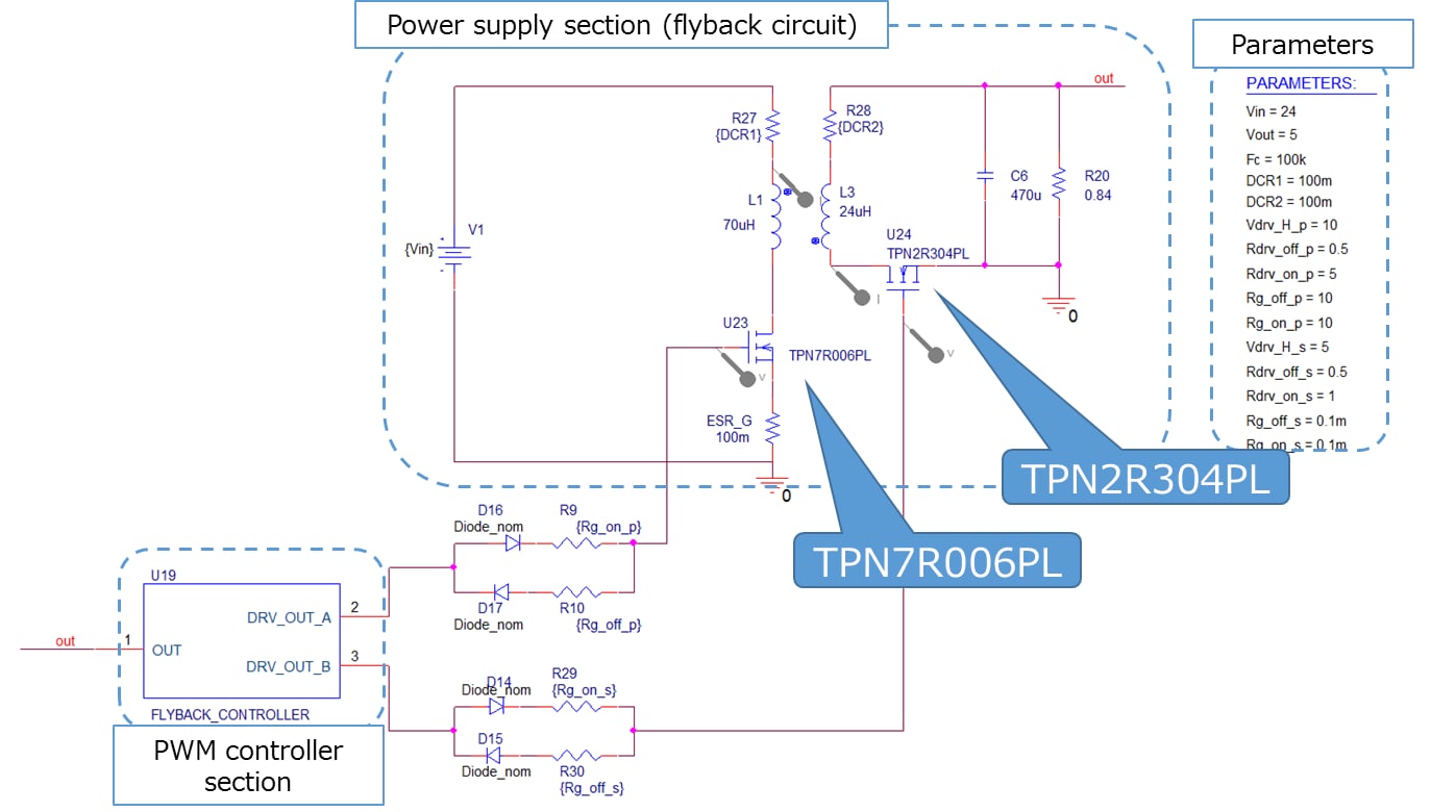
Circuit of flyback DC-DC power supply basic simulation circuit.
Flyback DC-DC Power Supply Basic Simulation Circuit
This reference design provides OrCAD® based simulation circuit, simulation results and design guide. This is for designing flyback topology of DC-DC power supply.
Design / Support / Reference Design Center
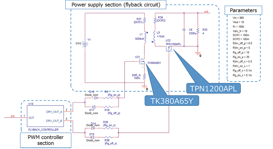
Circuit of flyback AC-DC power supply basic simulation circuit.
Flyback AC-DC Power Supply Basic Simulation Circuit
This reference design provides OrCAD® based simulation circuit, simulation results and design guide. This is for designing flyback topology of AC-DC power supply.
Flyback / AC-DC
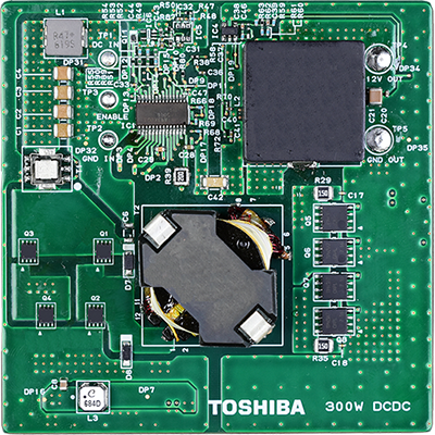
Features of 300W Isolated DC-DC converter.
300W Isolated DC-DC Converter
This reference design provides specification, block diagram and PCB layout data of 300W isolated DC-DC converter which is small size and suitable for consumer applications.
DC-DC Converter / Design / Support / Reference Design Center
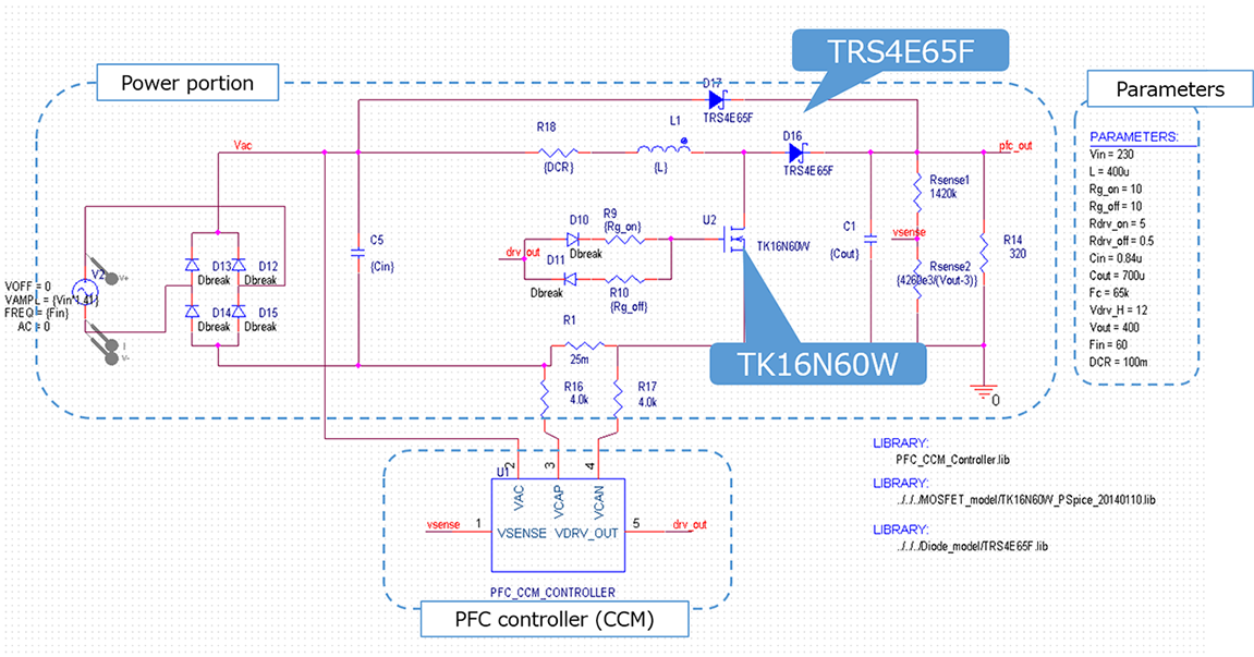
Circuit diagram of single phase PFC power supply basic simulation circuit.
Single Phase PFC Power Supply Basic Simulation Circuit
This reference design provides OrCAD® based simulation circuit, simulation results and design guide. This is for designing single phase PFC power supply.
Single Phase PFC Power Supply Basic Simulation Circuit
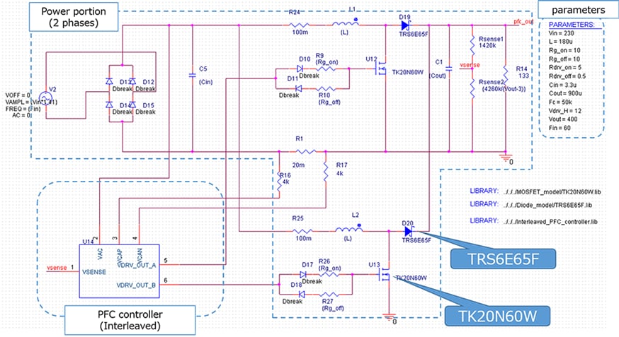
Circuit diagram of interleaved PFC power supply basic simulation circuit.
Interleaved PFC Power Supply Basic Simulation Circuit
This reference design provides OrCAD® based simulation circuit, simulation results and design guide. This is for designing interleaved PFC power supply.
Interleaved PFC Power Supply Basic Simulation Circuit
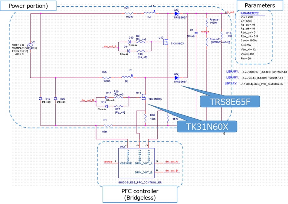
Circuit diagram of bridgeless PFC power supply basic simulation circuit.
Bridgeless PFC Power Supply Basic Simulation Circuit
This reference design provides OrCAD® based simulation circuit, simulation results and design guide. This is for designing bridgeless PFC power supply.
Bridgeless PFC Power Supply Basic Simulation Circuit
Block diagram of 200W AC-DC power supply.
200W AC-DC Power Supply
This reference design provides specification, block diagram and PCB layout data of DC24V/200W AC-DC power supply suitable for consumer applications and embedded power supply.
Semiconductor / power supply / power management / topology / flyback / AC-DC / MOSFET / diode
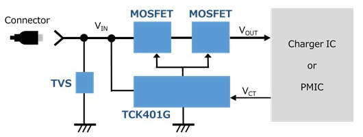
Battery charger circuit of MOSFET Driver IC application and circuit of the TCK401G.
MOSFET Driver IC Application and Circuit of the TCK401G
This reference design provides technical information on slew rate control, auto discharge and other built-in functions for designing load switch circuit suitable for USB-PD.
Semiconductor / power supply / power management / topology / flyback / AC-DC / MOSFET / diode
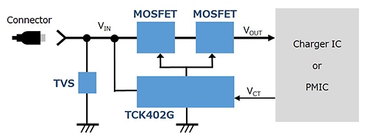
Battery charger circuit of MOSFET Driver IC application and circuit of the TCK402G.
MOSFET Driver IC Application and Circuit of the TCK402G
This reference design provides technical information on slew rate control, auto discharge and other built-in functions for designing load switch circuit suitable for USB-PD.
Semiconductor / power supply / power management / topology / flyback / AC-DC / MOSFET / diode
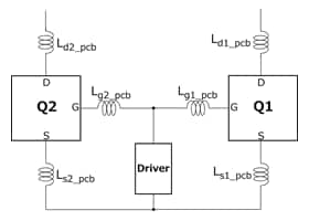
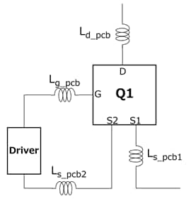
Device and prastic inductance of PCB trace of parallel operation of MOSFET(TPH1R306PL) application circuit.
Parallel Operation of MOSFET(TPH1R306PL) Application Circuit
This reference design provides example of simulation models/circuit and results for parallel operation using 60V MOSFET to increase output power.
Semiconductor / power supply / power management / topology / flyback / AC-DC / MOSFET / diode
Device and prastic inductance of PCB trace of parallel operation of MOSFET(TK62N60X) application circuit.
Parallel Operation of MOSFET(TK62N60X) Application Circuit
This reference design provides example of simulation models/circuit and results for parallel operation using 600V MOSFET to increase output power.
Semiconductor / power supply / power management / topology / flyback / AC-DC / MOSFET / diode
Device and prastic inductance of PCB trace of MOSFET 4 leads package TO-247-4L(TK25Z60X) application circuit.
MOSFET 4 Leads Package TO-247-4L(TK25Z60X) Application Circuit
This reference design provides example circuit for maximize switching performance and efficiency using 4 lead MOSFET package (TO-247-4L) which reduces package inductance.
Design / Support / Reference Design Center
Device and prastic inductance of PCB trace of MOSFET4 leads package DFN8x8(TK25V60X) application circuit.
MOSFET4 Leads Package DFN8x8(TK25V60X) Application Circuit
This reference design provides example circuit for maximize switching performance and efficiency using 4 lead MOSFET package (DFN8x8) which reduces package inductance.
Semiconductor / power supply / power management / topology / flyback / AC-DC / MOSFET / diode
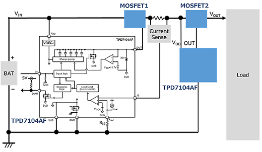
Short circuit detection circuit block diagram of single-output High-Side N-Channel Power MOSFET Gate Driver application and circuit of the TPD7104AF.
Single-Output High-Side N-Channel Power MOSFET Gate Driver Application and Circuit of the TPD7104AF
This reference design provides examples of application circuit and simulation for TPD7104AF which features short load protection, reverse power connection protection and others.
Semiconductor / Design & Development / Reference Design Center / Battery Management
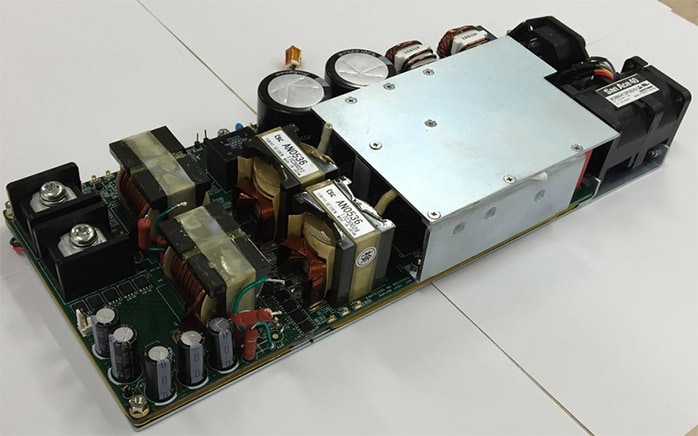
Features of 1.6kW, 80Plus Platinum class, high efficiency server AC-DC power supply .
1.6kW, 80Plus Platinum Class, High efficiency Server AC-DC Power supply
This reference design provides design guide, data and other contents of 1.6kW 80Plus Platinum class power supply using Semi-bridgeless/Isolated phase shift full bridge.
Semiconductor / power supply / power management / topology / flyback / AC-DC / MOSFET / diode / Toshiba
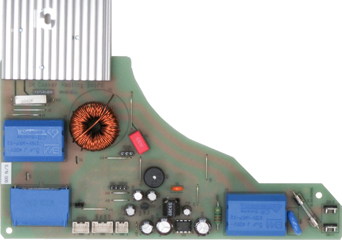
Photo of Inverter Circuit for IH Cooker
Inverter Circuit for IH Cooker
This reference design provides design guide, data and other contents of Inverter Circuit for IH Cooker based on Voltage-Resonant Soft Switching .
Low EMI Switching
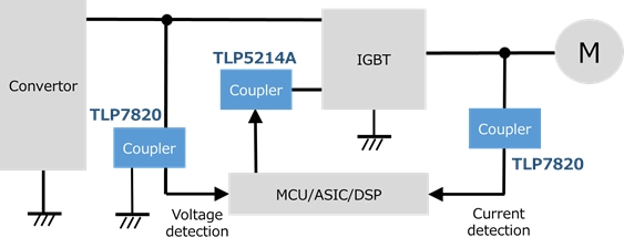
Inverter application example of smart gate driver coupler TLP5214A inverter application.
Smart Gate Driver Coupler TLP5214A Inverter Application
This reference design provides example circuits, design guide of built-in functions and thermal design guide for applying TLP5214A to inverter circuit as gate driver.
PCB Photo (example)
1.6 kW Server Power Supply (Upgraded)
Thanks to Toshiba’s latest power devices and digital isolator, this 1U size and 12 V output 1.6 kW server power supply achieves higher efficiency at whole load than the existing reference design which uses the same circuit topology. Design files and guides for circuit design and operation are available as reference design.
PCB photo example of Power multiplexer circuit
Power Multiplexer Circuit Using Common-Drain MOSFET
This power multiplexer circuit with 2 inputs and 1 output is realized on a small board. A new power multiplexer circuit usign common-drain MOSFET has been added to the already developed power multiplexer circuit reference design. These reference circuits allow switching between BBM and MBB modes by combining optimal devices such as MOSFET gate driver ICs and zener diodes from our diverse product lineup.
Power multiplexer circuit / 2 input and 1 output
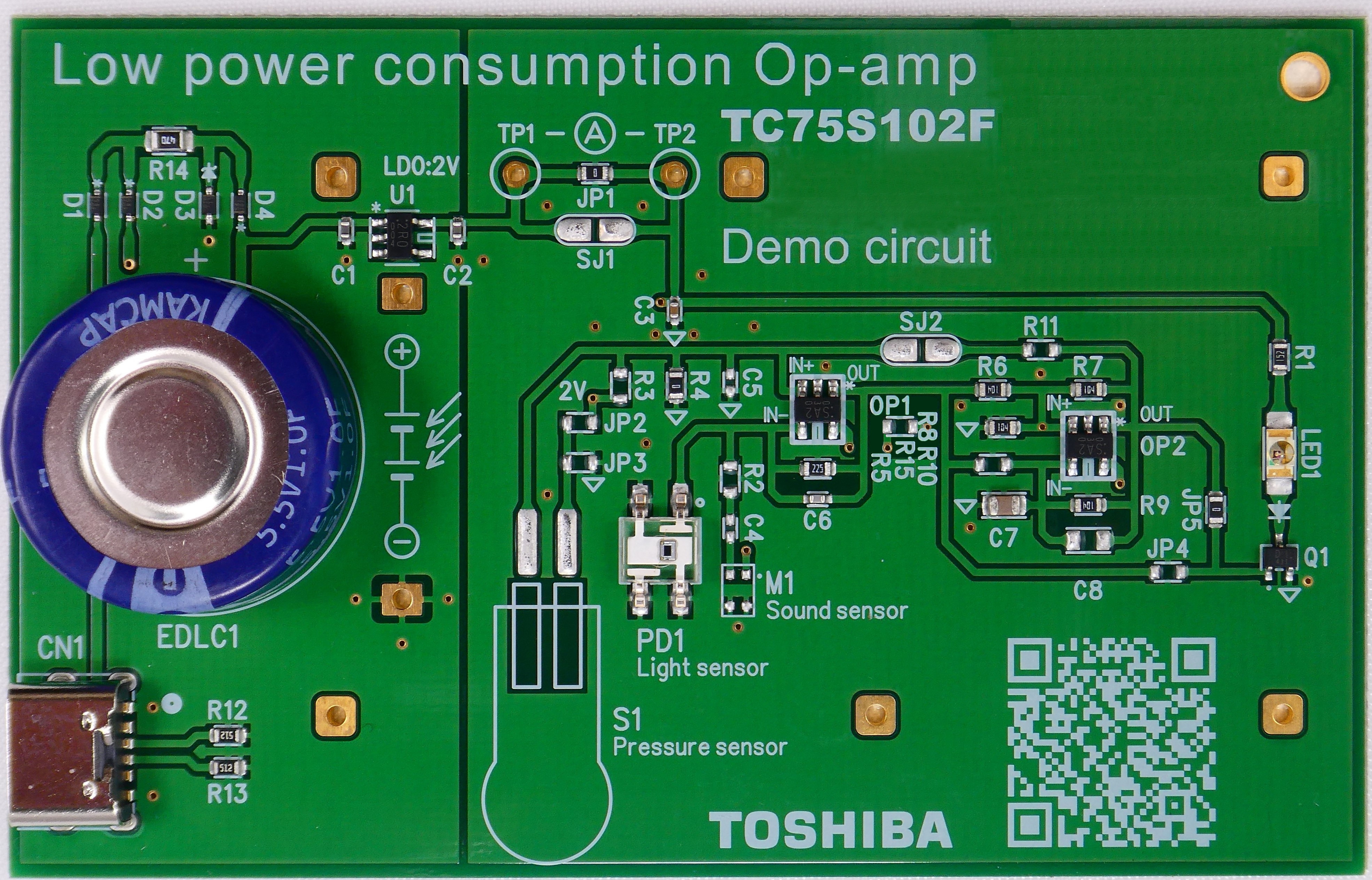
PCB Photo (example)
Application Circuit of Low Power Consumption Op-Amp TC75S102F
Application circuits of low power consumption Op-Amp TC75S102F for use with various sensors. These application circuits can be used for devices requiring long battery life, IoT sensor, energy harvesting, etc.
1.6 kW T-Type 3-Level PFC Power Supply
This reference design provides design guide, data and other contents of 1.6kW AC-DC converter power supply using T-Type 3-Level power factor correction (PFC) circuit.
PCB photo example of Power multiplexer circuit
Power multiplexer circuit
In this reference design, a Power multiplexer circuit with 2 input and 1 output is implemented on a small PCB. MOSFET gate driver ICs, eFuse ICs, zener diodes and small package MOSFETs selected from Toshiba's diverse lineup are used create ideal diode like characteristics with BBM and MBB switching.
Power multiplexer circuit / 2 input and 1 output
Features of 1.2V/100A output DC-DC converter compliant with 48V bus voltage.
1.2V/100A Output DC-DC Converter Compliant with 48V Bus Voltage
This reference design provides specification, block diagram and PCB layout data of 1.2V/100A output isolated DC-DC converter which convert 48V bus voltage to 1.2V directly.
DC-DC / MOSFET / reference design
Features of 300W Isolated DC-DC converter.
300W Isolated DC-DC Converter
This reference design provides specification, block diagram and PCB layout data of 300W isolated DC-DC converter which is small size and suitable for consumer applications.
DC-DC Converter / Design / Support / Reference Design Center
Circuit diagram of single phase PFC power supply basic simulation circuit.
Single Phase PFC Power Supply Basic Simulation Circuit
This reference design provides OrCAD® based simulation circuit, simulation results and design guide. This is for designing single phase PFC power supply.
Single Phase PFC Power Supply Basic Simulation Circuit
Circuit diagram of interleaved PFC power supply basic simulation circuit.
Interleaved PFC Power Supply Basic Simulation Circuit
This reference design provides OrCAD® based simulation circuit, simulation results and design guide. This is for designing interleaved PFC power supply.
Interleaved PFC Power Supply Basic Simulation Circuit
Circuit diagram of bridgeless PFC power supply basic simulation circuit.
Bridgeless PFC Power Supply Basic Simulation Circuit
This reference design provides OrCAD® based simulation circuit, simulation results and design guide. This is for designing bridgeless PFC power supply.
Bridgeless PFC Power Supply Basic Simulation Circuit
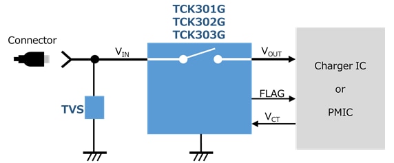
Main switch of a rapid-charging circuit of load switch IC TCK301G, TCK302G, TCK303G application & circuit.
Load Switch IC TCK301G, TCK302G, TCK303G Application & Circuit
This reference design provides example circuit of the load switch with low on resistance and built-in in-rush current control function. It is suitable for battery used application.
Load Switch IC / Application & Circuit
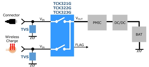
Battery charger circuit of load switch IC TCK321G, TCK322G, TCK323G application & circuit.
Load Switch IC TCK321G, TCK322G, TCK323G Application & Circuit
This reference design provides document with input selection characteristics. The load switch has small package and low on resistance suitable for battery charging application.
Load Switch IC / Application & Circuit / Design / Support / Reference Design Center
Features of 1.6kW, 80Plus Platinum class, high efficiency server AC-DC power supply .
1.6kW, 80Plus Platinum Class, High efficiency Server AC-DC Power supply
This reference design provides design guide, data and other contents of 1.6kW 80Plus Platinum class power supply using Semi-bridgeless/Isolated phase shift full bridge.
Semiconductor / power supply / power management / topology / flyback / AC-DC / MOSFET / diode / Toshiba

News / Latest information

Related FAQs

SiC MOSFETs

SiC Schottky Barrier Diodes

A new window will open