-
My ToshibaSemicon
- 반도체 탑
-
애플리케이션Automotive
Body Electronics
xEV
In-Vehicle Infotainment
Advanced Driver-Assistance Systems (ADAS)
Chassis
IndustrialInfrastructure
BEMS/HEMS
Factory Automation
Commercial Equipment
Consumer/PersonalIoT Equipment
Healthcare
Wearable Device
Mobile
Computer Peripherals
-
제품자동차 디바이스
Discrete Semiconductor
다이오드
트랜지스터
로직 IC
Analog Devices
Digital Devices
Wireless Devices
※
 : Products list (parametric search)파워반도체
※
: Products list (parametric search)Isolators/Solid State RelaysPhotocouplers
Digital Isolators
Solid State Relays
Fiber Optic Transmitting Modules
※
: Products list (parametric search)MOSFETsIGBTs/IEGTs바이폴라 트랜지스터※
: Products list (parametric search)다이오드※
: Products list (parametric search)마이크로컨트롤러모터 드라이버 ICIntelligent Power ICs※
: Products list (parametric search)전원관리IC리니어 IC※
: Products list (parametric search)범용로직IC리니어 이미지 센서기타 제품용 IC기타 제품용 IC
※
: Products list (parametric search) -
개발/설계 지원
-
기술 자료
- 구매처


- 부품 번호 & 키워드 검색
- 상호 참조 검색
- 파라미터 검색
- 재고 확인 및 구매
This webpage doesn't work with Internet Explorer. Please use the latest version of Google Chrome, Microsoft Edge, Mozilla Firefox or Safari.
3글자 이상 입력하세요. Search for multiple part numbers fromhere.
The information presented in this cross reference is based on TOSHIBA's selection criteria and should be treated as a suggestion only. Please carefully review the latest versions of all relevant information on the TOSHIBA products, including without limitation data sheets and validate all operating parameters of the TOSHIBA products to ensure that the suggested TOSHIBA products are truly compatible with your design and application.Please note that this cross reference is based on TOSHIBA's estimate of compatibility with other manufacturers' products, based on other manufacturers' published data, at the time the data was collected.TOSHIBA is not responsible for any incorrect or incomplete information. Information is subject to change at any time without notice.
3글자 이상 입력하세요.
Is it possible to leave the unused inputs of the general purpose logic ICs open?
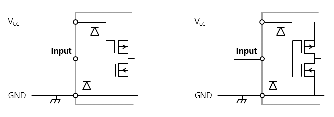
Generally, all unused inputs should be tied to either VCC or GND. (Fig. 1) The reason is that the input impedance of general-purpose logic ICs is extremely high, and if left open, an unintended value may be output due to the influence of the surrounding electric field. In addition, at the midpoint potential, through current flows and current consumption increases, and in some cases, it may lead to destruction of the element.
If the input pin does not have a bus hold function and there is no special description in the data sheet, take the above action.
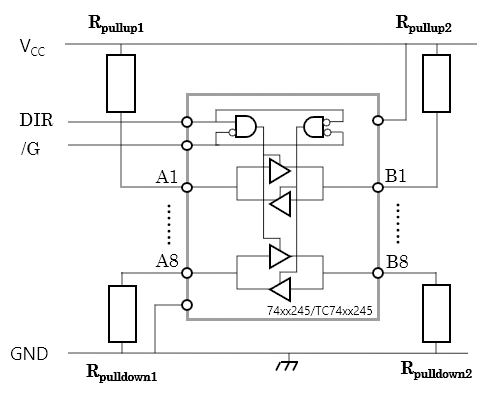
However, for pins (bus pins, etc.) that have the potential to become outputs like bi-directional bus buffers such as the 245, connect both ends of the input/output to the power supply or GND via pull-up/pull-down resistors. (Fig. 2)
It is recommended that both ends of the buffer be pulled up or down to the same potential to avoid unnecessary current flow. However, leave the input pins with bushold, such as those of the ICs of the TC74VCXHxxx Series, open. Large inrush current due to parasitic capacitance (in the order of a few milliamperes) can be a problem even with typical general-purpose ICs when their power supply is on. In order to improve system reliability against device destruction and other failures, their inputs can be tied to VCC via a pull-up resistor or to GND via a pull-down resistor.
Related Links
The following documents also contain related information.