-
My ToshibaSemicon
- 반도체 탑
-
애플리케이션Automotive
Body Electronics
xEV
In-Vehicle Infotainment
Advanced Driver-Assistance Systems (ADAS)
Chassis
IndustrialInfrastructure
BEMS/HEMS
Factory Automation
Commercial Equipment
Consumer/PersonalIoT Equipment
Healthcare
Wearable Device
Mobile
Computer Peripherals
-
제품자동차 디바이스
Discrete Semiconductor
다이오드
트랜지스터
로직 IC
Analog Devices
Digital Devices
Wireless Devices
※
: Products list (parametric search)
파워반도체※
: Products list (parametric search)
Isolators/Solid State RelaysPhotocouplers
Digital Isolators
Solid State Relays
Fiber Optic Transmitting Modules
※
: Products list (parametric search)
MOSFETsIGBTs/IEGTs바이폴라 트랜지스터※
: Products list (parametric search)
다이오드※
: Products list (parametric search)
마이크로컨트롤러모터 드라이버 ICIntelligent Power ICs※
: Products list (parametric search)
전원관리IC리니어 IC※
: Products list (parametric search)
범용로직IC리니어 이미지 센서기타 제품용 IC기타 제품용 IC
※
: Products list (parametric search)
-
개발/설계 지원
-
기술 자료
- 구매처
- 부품 번호 & 키워드 검색
- 상호 참조 검색
- 파라미터 검색
- 재고 확인 및 구매
This webpage doesn't work with Internet Explorer. Please use the latest version of Google Chrome, Microsoft Edge, Mozilla Firefox or Safari.
3글자 이상 입력하세요. Search for multiple part numbers fromhere.
The information presented in this cross reference is based on TOSHIBA's selection criteria and should be treated as a suggestion only. Please carefully review the latest versions of all relevant information on the TOSHIBA products, including without limitation data sheets and validate all operating parameters of the TOSHIBA products to ensure that the suggested TOSHIBA products are truly compatible with your design and application.Please note that this cross reference is based on TOSHIBA's estimate of compatibility with other manufacturers' products, based on other manufacturers' published data, at the time the data was collected.TOSHIBA is not responsible for any incorrect or incomplete information. Information is subject to change at any time without notice.
3글자 이상 입력하세요.
Gate Driver IC for Automotive Brushed Motors
This is a 2ch half-bridge (H-bridge) gate driver IC with the minimum functions required for automotive applications.
Compatible with body systems in general that use brushed motors.
In particular, by converting a system that uses mechanical relays to drive motors to semiconductors, high reliability and miniaturization can be achieved.
<Points of this product>
- Contributing to Simplified System Design with Compact Functions
- Use of small packages (VQFN24) to help reduce the size of ECU's [Note 1]
- Contributes to switching from mechanical relays to semiconducting (MOSFET)
In recent years, there has been an increase in the demand for motors per vehicle due to the increasingly electrified moving parts of automotive equipment, which had been mechanical. The number of drivers driving motors is also increasing, and the system is becoming smaller and more integrated. Some motor applications require no rotational speed control, and a driver with limited functions and performance is required.
We are working to strengthen our product lineup to meet this demand, and TB9103FTG introduced here is part of this enhancement (Table 1).
Table 1. Lineup of Gate Driver IC for Automotive Brushed Motors
GD: Gate Driver, CP: Charge Pump, MCSA: Motor Current Sense Amplifier, SR: Safety Relay, Dev.: Development, xTBV: x Times Battery Voltage
| Part number | Status | Package | GD | CP | MC SA |
GD for SR |
SPI | Comment |
|---|---|---|---|---|---|---|---|---|
| TB9103FTG | MP | VQFN24 | ○ (H-bridge or 2ch Half-bridge) |
○ (2TBV) |
- | - | - | Propose to replace mechanical relay by semiconductor relay. |
| TB9104FTG | Dev. | VQFN32 | ○ (H-bridge or 2ch Half-bridge) |
○ (2TBV) |
○ (1ch) |
○ (1ch) |
○ |
Highly general purpose device with minimum functionality. |
| TB9052FNG | MP | HTSSOP48 | ○ (H-bridge) |
○ (3TBV) |
○ (1ch) |
- | - | Built-in motor control profile. |
| TB9057FG | MP | LQFP48 | ○ (H-bridge) |
○ (3TBV) |
○ (1ch) |
- | - | Operation under low battery voltage, Enhanced FuSa. Built-in Phase Monitor to monitor direction of motor operation. |
Equipped with the minimum necessary functions for automotive applications
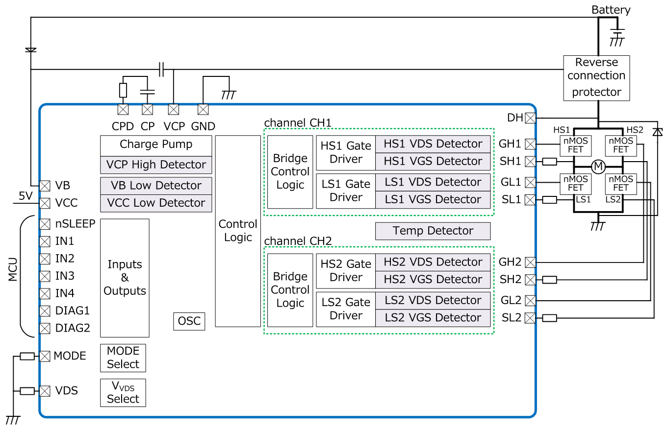
TB9103FTG is a gate-driver IC for controlling the external Nch-MOSFET that drives the brushed motors. In addition, various abnormal conditions (VDS, VGS, overtemperature, power supply, setting, etc.) are outputted at DIAG terminal. There are two DIAG jacks, which can be used to determine which channel of a half-bridge with two channels has an error.

TB9103FTG value ①:
Contributing to Simplified System Design with Compact Functions
TB9103FTG assumes that a microcomputer that enables high-level control is not used, but the through-current of external Nch-MOSFETs, which is the most important factor to avoid in a system, is avoided by the product's built-in automatic dead-time control.
TB9103FTG value ②:
Use of small packages (VQFN24) to help reduce the size of ECU's [Note 1]
The TB9103FTG has reduced the number of terminals by downsizing the functions, enabling the selection of a package that is among the smallest in the world. [Note 2]
Its dimensions are 16mm2 in 24pin of VQFN.

The QFN package is used to realize the small size of this product. Also, by hiding the corner pins that have GND potential in the mold resin, the risk of malfunctions due to short failures between pins is reduced.
TB9103FTG value ③:
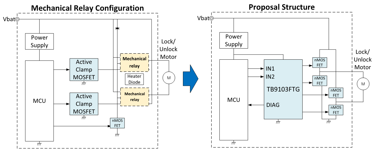
Contributes to switching from mechanical relays to semiconducting (MOSFET)
Advantages of switching from mechanical relays to semiconductors (MOSFETs) include quiet operation (no relay noise), high reliability (long life), and small size (small mounting area).
The following figure (Figure 3) illustrates the image.

TB9103FTG major specifications
The power supply (VB, VCC) is intended for use with a 12V battery system. The guaranteed chip temperature range is -40℃ to 150℃, which corresponds to Grade1 in the AEC-Q100 [NOTE 3].
This product is equipped with a charge pump that can drive an external Nch-MOSFET. The main specifications are shown below (Table 2).
Operating voltage range (excerpt)
| Item | Symbol | Terminal | Limit Values | ||
|---|---|---|---|---|---|
| Min | Max | Unit | |||
| Power supply voltage operating range 1 | VCCrng | VCC | 4.5 | 5.5 | V |
| Power supply voltage operating range 2 | VBrng | VB | 7 | 18 | V |
Electrical Characteristics (extract)
Unless otherwise specified, VB=7 to 18V, VCC=4.5 to 5.5V (VB≧VCC) and Ta=-40 to 125℃.
| Item | Symbol | Terminal | Limit Values | |||
|---|---|---|---|---|---|---|
| Min | Typ. | Max | Unit | |||
| Charge pump voltage | VCP1 | VCP | VB+5 | VB+11 | VB+14 | V |
| Between the high-side GSs Drive voltage |
VGSHSSRC1 | GH1, GH2 | VCP-VB -0.2 |
- | VCP-VB | V |
| VGSHSSNK1 | GH1, GH2 | - | - | 0.5 | V | |
| Between the low-side GSs Drive voltage |
VGSLSSRC1 | GL1, GL2 | 8.9 | 11 | 14 | V |
| VGSLSSRC2 | GL1, GL2 | VB-0.1 | - | VB | V | |
| VGSLSSNK1 | GL1, GL2 | - | - | 0.5 | V | |
| Between the high-side GSs Drive output resistance Source direction |
Ronhssrc | GH1, GH2 | 250 | 500 | 1000 | Ω |
| Between the high-side GSs Drive output resistance Sink direction |
Ronhssnk | GH1, GH2 | 20 | 50 | 150 | Ω |
| Between the low-side GSs Drive output resistance Source direction |
Ronlssrc | GL1, GL2 | 250 | 500 | 1000 | Ω |
| Between the low-side GSs Drive output resistance Sink direction |
Ronlssnk | GL1, GL2 | 20 | 50 | 150 | Ω |
Setting
MODE setting:
Two types of mode selectable: H-bridge mode /Half-bridge mode
VDS Detect Level Setting:
This is the setting of the function to monitor abnormalities in the drain-source voltage of external Nch-MOSFETs.
The detection level can be set in 4 steps (disable function, 0.3V, 0.6V, 0.9V).
Free loan of product evaluation boards
To enable customers to easily verify the characteristics of the TB9084FTG, we provide evaluation boards on free of charge. Of course, engineering samples can be submitted. Please contact our sales staff or our business partners at your service.
The size of the evaluation board is 95mm×75mm.
For customer convenience, switches, jumpers, and connectors are mounted as appropriate.
Toshiba is currently working to enhance a product lineup of ICs that control motors for automotive equipment. We will contribute to the electrification of automotive equipment and the improvement of comfort by introducing products to the market that optimize the functions and performance built into ICs to meet customers' needs.
[Note 1] Abbreviation for Electronic Control Unit, a device in which electronic components are mounted on a board.
[Note 2] According to our research in April 2022.
[Note 3] Reliability testing and other standards for automotive ICs defined by the Automotive Electronics Council.
Related information
Queries about purchasing, sampling and IC reliability
재고 확인 및 구매
3글자 이상 입력하세요.
Through this website you are able to proceed to the website of our distributors ("Third Party Website") which is not under the control of Toshiba Corporation and its subsidiaries and affiliates (collectively "Toshiba"). The Third Party Website is made available to you as a convenience only and you agree to use the Third Party Website at your own risk. The link of the Third Party Website does not necessarily imply a recommendation or an endorsement by Toshiba of the Third Party Website. Please be aware that Toshiba is not responsible for any transaction done through the Third Party Website, and such transactions shall be subject to terms and conditions which may be provided in the Third Party Website.
* Company names, product names, and service names may be trademarks of their respective companies.

