
-
My ToshibaSemicon
- 반도체 탑
-
애플리케이션Automotive
Body Electronics
xEV
In-Vehicle Infotainment
Advanced Driver-Assistance Systems (ADAS)
Chassis
IndustrialInfrastructure
BEMS/HEMS
Factory Automation
Commercial Equipment
Consumer/PersonalIoT Equipment
Healthcare
Wearable Device
Mobile
Computer Peripherals
-
제품자동차 디바이스
Discrete Semiconductor
다이오드
트랜지스터
로직 IC
Analog Devices
Digital Devices
Wireless Devices
※
 : Products list (parametric search)파워반도체
※
: Products list (parametric search)Isolators/Solid State RelaysPhotocouplers
Digital Isolators
Solid State Relays
Fiber Optic Transmitting Modules
※
: Products list (parametric search)MOSFETsIGBTs/IEGTs바이폴라 트랜지스터※
: Products list (parametric search)다이오드※
: Products list (parametric search)마이크로컨트롤러모터 드라이버 ICIntelligent Power ICs※
: Products list (parametric search)전원관리IC리니어 IC※
: Products list (parametric search)범용로직IC리니어 이미지 센서기타 제품용 IC기타 제품용 IC
※
: Products list (parametric search) -
개발/설계 지원
-
기술 자료
- 구매처


- 부품 번호 & 키워드 검색
- 상호 참조 검색
- 파라미터 검색
- 재고 확인 및 구매
This webpage doesn't work with Internet Explorer. Please use the latest version of Google Chrome, Microsoft Edge, Mozilla Firefox or Safari.
3글자 이상 입력하세요. Search for multiple part numbers fromhere.
The information presented in this cross reference is based on TOSHIBA's selection criteria and should be treated as a suggestion only. Please carefully review the latest versions of all relevant information on the TOSHIBA products, including without limitation data sheets and validate all operating parameters of the TOSHIBA products to ensure that the suggested TOSHIBA products are truly compatible with your design and application.Please note that this cross reference is based on TOSHIBA's estimate of compatibility with other manufacturers' products, based on other manufacturers' published data, at the time the data was collected.TOSHIBA is not responsible for any incorrect or incomplete information. Information is subject to change at any time without notice.
3글자 이상 입력하세요.
3rd generation SiC MOSFETs that contributes to lower loss of power supply in application
Power devices are essential components for managing and reducing power consumption in all kinds of electronic equipment, and for achieving a carbon neutral society. SiC is widely seen as the next generation material for power devices, as it delivers higher voltages and lower losses than silicon. While SiC power devices are now mainly utilized in inverters for trains, wider application is on the horizon, in vehicle electrification and the miniaturization of industrial equipment. However, the adoption and market growth of SiC devices have been held back by reliability issues.
Therefore, our 3rd generation SiC MOSFETs have the following features.
- Built-in Schottky barrier diode (SBD) reduced the forward voltage VDSF , and suppresses fluctuation in on-resistance RDS(ON)
- The performance index RDS(ON) × Qgd, which shows the relation between conduction loss and switching loss, is reduced
- Wide gate-source voltage VGSS specification range
Toshiba's 3rd generation SiC MOSFETs have a lineup of 650 V and 1200 V voltage products and provides lower loss of power supply for applications such as servers, uninterruptible power supplies (UPS), Photovoltaics Inverter.
The features of our 3rd generation SiC MOSFETs are introduced in detail below.
Features of the 3rd Generation SiC MOSFETs
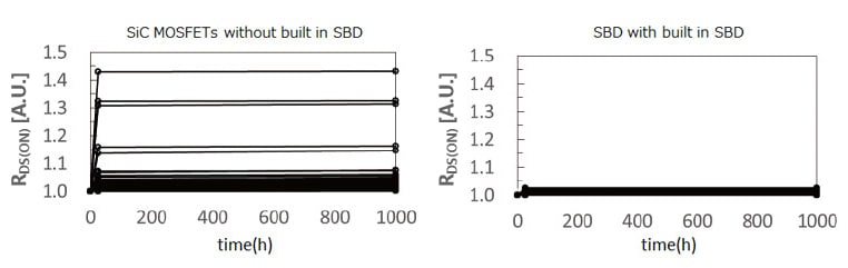
1. Built-in Schottky barrier diode (SBD) reduces VDSF and suppresses fluctuation in on-resistance RDS(ON)
Our 3rd-generation SiC MOSFET has a built-in Schottky barrier diode (SBD) in parallel with the PN diode that exists between the drain and source, so built-in Schottky barrier diode reduces the forward voltage VDSF during reverse conduction to 1.35 V (typ.).
By energizing the SBD, we suppress fluctuation of the on-resistance RDS(ON) between the drain and source caused by the spread of defects in the SiC crystal.
When a current density of 250 A/cm2 was applied from the source to the drain for 1000 hours, the on-resistance RDS(ON) of the SiC MOSFET without the built-in SBD was 42 % at maximum because the body diode was energized.
On the other hand, in the 3rd generation SiC MOSFETs with built-in SBD, we were able to suppress the fluctuation of on-resistance RDS(ON) to a maximum of 3 % because the SBD can be energized.
2. Reduced the conduction loss and switching loss performance index : RDS(ON) × Qgd
For our 3rd-generation SiC MOSFETs, the performance index RDS(ON) × Qgd, which shows the relation between conduction loss and switching loss, is reduced by 80 % [note] compared with our existing 2nd-generation products by optimizing its cell structure.
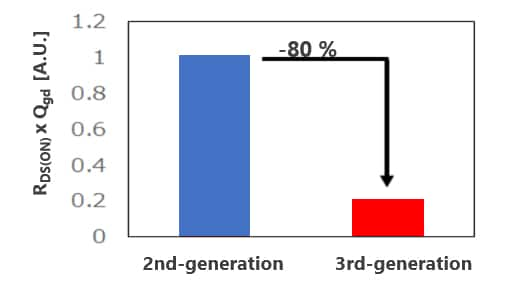
Measurement conditions
RDS(ON): VGS = 18 V, ID = 20 A, Ta = 25℃
Qgd: VDD = 800 V, VGS = 18 V, ID = 20 A, Ta = 25℃
(Toshiba internal comparison, as of May 2022)
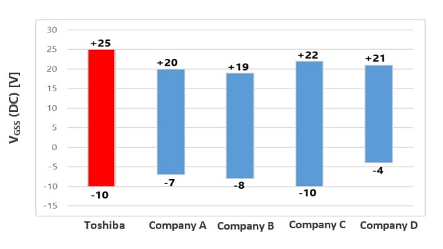
3. Wide gate-source voltage VGSS specification range
For our 3rd-generation SiC MOSFETs, the specification range of the gate-source voltage is -10 to 25 V, which is wider than that of other companies' products, allows a wider margin for the drive voltage and makes gate drive design easier. (Recommended drive voltage: VGS_on = 18 V, VGS_off = 0 V)
[Note] Comparison of our 1200 V 3rd generation SiC MOSFETs when RDS(ON) × Qgd is set to 1 in our 2nd generation SiC MOSFETs is set to 1.
SiC MOSFETs
Related information
See the following pages for various applications.
Server
Uninterruptible Power Supply
LED Lighting
See the following page for various application notes.
Features of third generation SiC MOSFET (PDF: 1,318KB)
FAQ: SiC MOSFET Application Notes (PDF: 818KB)
Comparison of SiC MOSFET and Si IGBT: SiCMOSFET Application Notes (PDF: 922KB)
Absolute Maximum Ratings and Electrical Characteristics: SiCMOSFET Application Notes (PDF: 812KB)
자주 있는 문의
See the following page for frequently asked questions.
MOSFETs
Simulation Model
You can use various simulation models.
* PSpice® is a registered trademark of Cadence Design Systems, Inc.
* LTspice® is simulation software and registered trademarks of Analog Devices, Inc.
* SIMetrix® is simulation software and registered trademarks of SIMetrix Technologies Ltd.
* Other company names, product names, and service names may be trademarks of their respective companies.