-
My ToshibaSemicon
- 반도체 탑
-
애플리케이션Automotive
Body Electronics
xEV
In-Vehicle Infotainment
Advanced Driver-Assistance Systems (ADAS)
Chassis
IndustrialInfrastructure
BEMS/HEMS
Factory Automation
Commercial Equipment
Consumer/PersonalIoT Equipment
Healthcare
Wearable Device
Mobile
Computer Peripherals
-
제품자동차 디바이스
Discrete Semiconductor
다이오드
트랜지스터
로직 IC
Analog Devices
Digital Devices
Wireless Devices
※
: Products list (parametric search)
파워반도체※
: Products list (parametric search)
Isolators/Solid State RelaysPhotocouplers
Digital Isolators
Solid State Relays
Fiber Optic Transmitting Modules
※
: Products list (parametric search)
MOSFETsIGBTs/IEGTs바이폴라 트랜지스터※
: Products list (parametric search)
다이오드※
: Products list (parametric search)
마이크로컨트롤러모터 드라이버 ICIntelligent Power ICs※
: Products list (parametric search)
전원관리IC리니어 IC※
: Products list (parametric search)
범용로직IC리니어 이미지 센서기타 제품용 IC기타 제품용 IC
※
: Products list (parametric search)
-
개발/설계 지원
-
기술 자료
- 구매처
- 부품 번호 & 키워드 검색
- 상호 참조 검색
- 파라미터 검색
- 재고 확인 및 구매
This webpage doesn't work with Internet Explorer. Please use the latest version of Google Chrome, Microsoft Edge, Mozilla Firefox or Safari.
3글자 이상 입력하세요. Search for multiple part numbers fromhere.
The information presented in this cross reference is based on TOSHIBA's selection criteria and should be treated as a suggestion only. Please carefully review the latest versions of all relevant information on the TOSHIBA products, including without limitation data sheets and validate all operating parameters of the TOSHIBA products to ensure that the suggested TOSHIBA products are truly compatible with your design and application.Please note that this cross reference is based on TOSHIBA's estimate of compatibility with other manufacturers' products, based on other manufacturers' published data, at the time the data was collected.TOSHIBA is not responsible for any incorrect or incomplete information. Information is subject to change at any time without notice.
3글자 이상 입력하세요.
Contributes to downsizing of equipment and reduction of power consumption

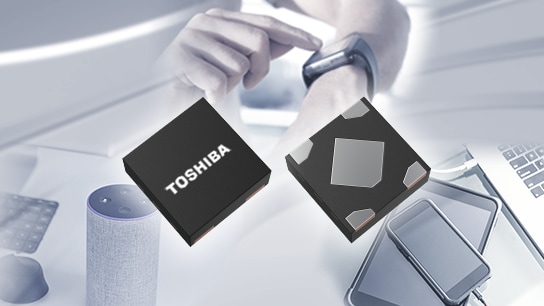
Toshiba Electronic Devices & Storage Corporation (“Toshiba”) start mass production of TCR3LM Series, low-current LDO regulators, packaged in DFN4D at Toshiba Semiconductor Thailand.
Demand for IoT communication modules and wearable devices and any mobiles is increasing. While batteries are getting smaller with the demand for initialization, longer battery life is required. In order to achieve long-term operation of the equipment, it is necessary to keep the power consumption of the equipment itself low. One of important things is to keep the current consumption low when devices are in the standby state. The battery will be in standby mode except during operations such as data transfer, but this standby mode will occupy most of the day.
In other words, by keeping the current consumption in this standby state low, it is possible to keep the current consumption of the device itself low, and as a result, it is possible to realize long-time operation even with a small battery capacity.
The new TCR3LM series-a LDO regulator with low current consumption-contributes to reduce the power consumption of equipment. Drop-out performance is improved compared to our another low current LDO TCR2LN series-type [Note 1]. TCR3LM series also offers improved load transient response. This enables more stable output against load fluctuations. In addition, we offer an extensive lineup of output voltage products. Since the max. output current is 300 mA, you can select the best device including our existing-product TCR2LN series. It can be used for a wide range of applications.
TCR3LM series are in surface-mount-type compact, low-profile DFN4D packaging. In addition, small ceramic types can be used for input and output capacitors, making them suitable for power supply lines for mobile devices, wearable devices, and other small devices that require high-density mounting.
[Note 1] Output-current 200 mA
Features
- Low Current Consumption (Low Bias Current): IB(ON)=2.2 μA (max) (IOUT=0 mA, Vin=5.5 V)
- Low dropout voltage: VDO=344 mV (typ.) (VOUT=1.8 V, IOUT=200 mA)
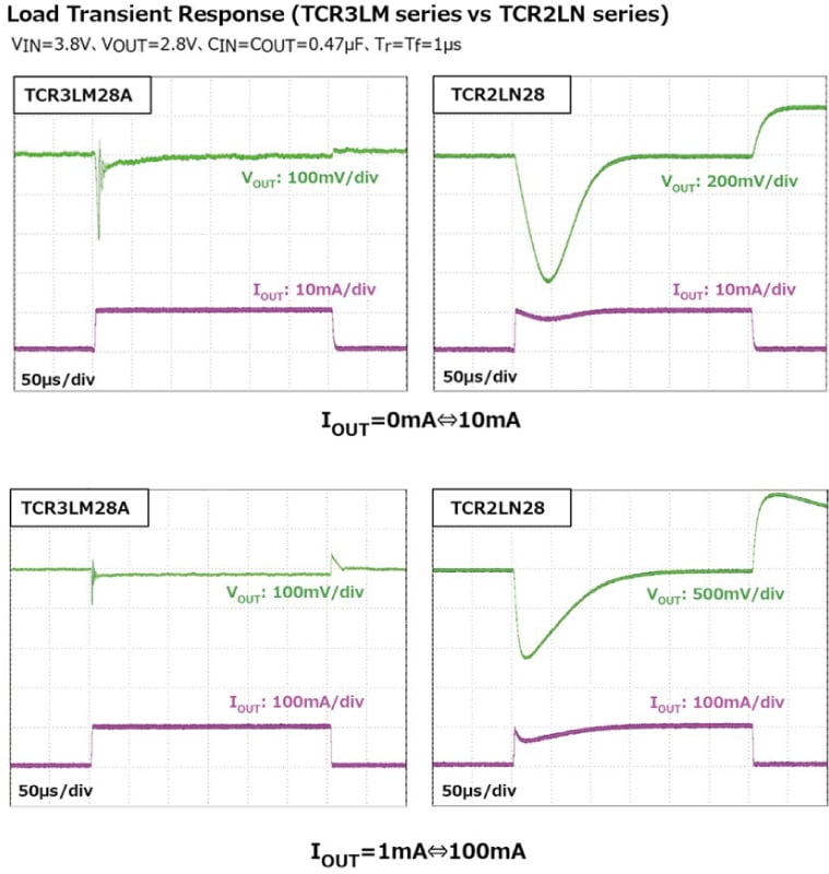
- Load Transient Response Characteristics: -70/+35 mV (typ.) (VOUT=2.8 V, IOUT=1 mA⇔100 mA)
1. Low Current Consumption (Low Bias Current): IB(ON)=2.2 μA (max) (IOUT=0 mA, Vin=5.5 V)
Bias current is the current that flows through the input of the LDO regulator when no output current flows, and the current is required to operate LDO regulator itselves. LDO regulator is used as a power supply for various functional blocks, such as various sensing and data communications. These functions are not always in operation, and some of them may not be in standby mode. In the standby mode, almost no current is supplied to LDO regulator output. Therefore, by making the operating times of the functions as short as possible, measures are taken to keep the average-consumption current (power) of the entire device low. In this case, only the bias current flows from the battery. This characteristic is important to reduce the current consumption. TCR3LM Series suppresses the biasing current to 2.2 μA (max), contributing to power saving and long-time driving of the entire equipment.
2. Low dropout voltage: VDO=344 mV (typ.) (VOUT=1.8 V, IOUT=200 mA)
TCR3LM Series has improved the dropout voltage compared to the conventional product while reducing the biasing current. Generally, decreasing the bias current will degrade the regulator performance. The TCR3LM series has succeeded in both reducing bias current and improving dropout voltage by reviewing the circuit configuration. Since the desired output voltage can be obtained at a lower input voltage than the conventional product, the power consumption can be reduced due to the voltage difference.
3. Load Transient Response Characteristics: -70/+35 mV (typ.) (VOUT=2.8 V, IOUT=1 mA⇔100 mA)
TCR3LM Series has improved the load-transient response-characteristics compared to the conventional product while reducing the biasing current. Generally, decreasing the bias current will degrade the regulator performance. A load transient response indicates the magnitude of output voltage fluctuation that occurs when the output current suddenly increases or decreases. There is a trade-off between reducing the biasing current and deteriorating this performance, but TCR3LM Series has succeeded in improving both by reviewing the circuitry.

애플리케이션
- Mobile devices
- Wearable terminal
- IoT Communication Modules
Main Specifications
(Unless otherwise specified, Ta=25 °C)
| Product Number | TCR2LN series[Note 2] | TCR3LM series | |||
|---|---|---|---|---|---|
| Package | Name | SDFN4 | DFN4D | ||
| Size (mm) | Typ. | 0.8×0.8, t=0.38 | 1.0×1.0, t=0.37 | ||
| Operating range (Ta=-40 to 85 °C) |
Input-voltage VIN (V) | 1.5 to 5.5 | 1.4 to 5.5 | ||
| Output-Voltage VOUT (V) | 0.8 to 3.6 | 0.8 to 5.0 | |||
| Output-current IOUT (mA) | 200 | 300 | |||
| Electrical characteristics (Unless otherwise specified, Tj=-40 to 85 °C) |
Biased current IB(ON) (μA) | Max | 2.0 (IOUT=0 mA, VIN=2.5 V [Note 3]) |
2.2 (IOUT=0 mA, VIN=5.5 V [Note 3]) |
|
| Dropout Voltage VDO (mV) | Max | 600 (IOUT=150 mA, VOUT=1.8 V) |
445 (IOUT=200 mA, VOUT=1.8 V) |
||
| Load-transient response⊿ VOUT (mV) |
Tj=25 °C | Typ. | -400/+400 (1⇔10 mA) |
-70/+35 (1⇔100 mA) |
|
| Control terminal Threshold voltage VCTH (V) |
Control terminal input-voltage "HIGH" |
Min | - | 0.9 | |
| Control terminal Threshold voltage VCTL (V) |
Control terminal input-voltage "LOW" |
Max | - | 0.4 | |
| Control-Voltage (ON) VCT (ON) | Min | 1.0 | - | ||
| Control-voltage (OFF) VCT (OFF) | Max | 0.4 | - | ||
| Overcurrent protection function | Yes | ||||
| Overheat protection function | Yes | ||||
| Auto discharge function | Yes | ||||
| Sample Check & Availability |  |
 |
|||
[Note 2] Existing products
[Note 3] Control pull-down current (ICT) is not included.
Related information
Product information
Application
FAQ
Queries about purchasing, sampling and IC reliability
재고 확인 및 구매
3글자 이상 입력하세요.
Through this website you are able to proceed to the website of our distributors ("Third Party Website") which is not under the control of Toshiba Corporation and its subsidiaries and affiliates (collectively "Toshiba"). The Third Party Website is made available to you as a convenience only and you agree to use the Third Party Website at your own risk. The link of the Third Party Website does not necessarily imply a recommendation or an endorsement by Toshiba of the Third Party Website. Please be aware that Toshiba is not responsible for any transaction done through the Third Party Website, and such transactions shall be subject to terms and conditions which may be provided in the Third Party Website.
* Company names, product names, and service names may be trademarks of their respective companies.
* Information in this document, including product prices and specifications, content of services and contact information, is current on the date of the announcement but is subject to change without prior notice.

