- General Top
- SEMICONDUCTOR
- STORAGE
- COMPANY
-
My ToshibaSemicon
- Semiconductor Top
-
ApplicationsAutomotive
Body Electronics
xEV
In-Vehicle Infotainment
Advanced Driver-Assistance Systems (ADAS)
Chassis
IndustrialInfrastructure
BEMS/HEMS
Factory Automation
Commercial Equipment
Consumer/PersonalIoT Equipment
Healthcare
Wearable Device
Mobile
Computer Peripherals
-
ProductsAutomotive Devices
Discrete Semiconductor
Diodes
Transistors
Logic ICs
Analog Devices
- Automotive SmartMCD™ (Integreted SoC Conbining Microcontroller and Driver)
- Automotive Brushless Motor Driver ICs
- Automotive Brushed DC Motor Driver ICs
- Automotive Stepping Motor Driver ICs
- Automotive Driver ICs
- Automotive System Power Supplies ICs
- Automotive audio power amplifier ICs
- Automotive Network Communication
Digital Devices
Wireless Devices
※
 : Products list (parametric search)Power Semiconductors
SiC Power Devices
※
: Products list (parametric search)Isolators/Solid State RelaysPhotocouplers
Digital Isolators
Solid State Relays
Fiber Optic Transmitting Modules
※
: Products list (parametric search)MOSFETsIGBTs/IEGTsBipolar Transistors※
: Products list (parametric search)Diodes※
: Products list (parametric search)MicrocontrollersMotor Driver ICsIntelligent Power ICs※
: Products list (parametric search)Power Management ICsLinear ICs※
: Products list (parametric search)General Purpose Logic ICsLinear Image SensorsOther Product ICsOther Product ICs
※
: Products list (parametric search) -
Design & Development
Design & Development
Innovation Centre
At the Toshiba Innovation Centre we constantly strive to inspire you with our technologies and solutions. Discover how to place us at the heart of your innovations.
-
Knowledge
Knowledge
Highlighted Topics
Further Materials
Other
- Where To Buy


- Part Number & Keyword Search
- Cross Reference Search
- Parametric Search
- Stock Check & Purchase
This webpage doesn't work with Internet Explorer. Please use the latest version of Google Chrome, Microsoft Edge, Mozilla Firefox or Safari.
require 3 characters or more. Search for multiple part numbers fromhere.
The information presented in this cross reference is based on TOSHIBA's selection criteria and should be treated as a suggestion only. Please carefully review the latest versions of all relevant information on the TOSHIBA products, including without limitation data sheets and validate all operating parameters of the TOSHIBA products to ensure that the suggested TOSHIBA products are truly compatible with your design and application.Please note that this cross reference is based on TOSHIBA's estimate of compatibility with other manufacturers' products, based on other manufacturers' published data, at the time the data was collected.TOSHIBA is not responsible for any incorrect or incomplete information. Information is subject to change at any time without notice.
require 3 characters or more.
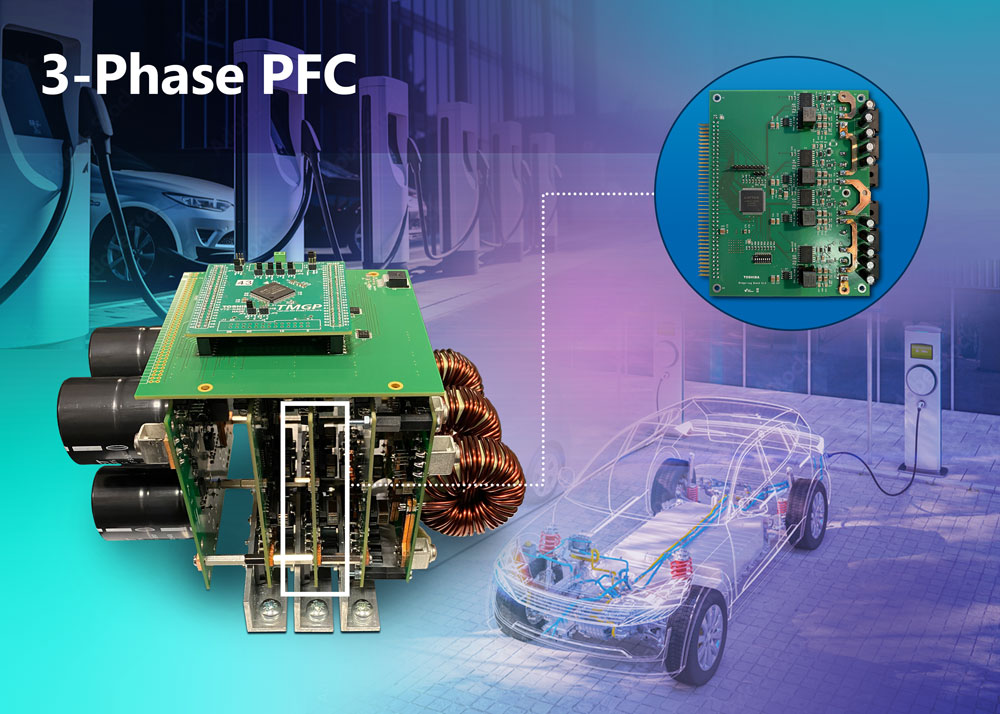
A different way to design high power charging solutions
Due to a combination of consumer demand and governmental policy to halt sales of new internal combustion engines (including in hybrid vehicles), all-electric battery electric vehicles (BEVs) are the future of personal mobility. In order to provide the performance and range needed to be successful a reliable, robust and efficient conversion of electrical energy is needed, especially for traction inverters and battery chargers.
Even though there are significant areas of similarity in the electronics required, designs have been carried out separately for the PFC, inverter and DC/DC converter. This approach is inefficient and involves significant repetition which, if eliminated, can reduce the design burden and bring chargers and vehicles to market more rapidly.
No matter the power level, almost all chargers have a common architecture encompassing a PFC stage followed by isolated DC/DC conversion and filtering. Delving deeper into the design, the topologies chosen are often the same and within these, circuit elements are often repeated.
For example PFC, dual active bridge (DAB) and LLC converters that are often used for charging contain multiple single bridge legs – a feature that is also used in motor inverters.
Leveraging this fact, Toshiba has reimagined the design process and developed the Modular EV Charger PFC Reference Design Concept – known as their ‘SiC Cube’.
This innovative design comprises seven PCBs that combine to create a very compact PFC solution. The central three boards are the bridge legs common to all mentioned circuits. They are designed in a 3-level NPC topology using SiC MOSFETs, SiC diodes and isolated gate drivers.
The remaining boards are input inductor and output capacitor boards (with current and voltage measurement), the signal connecting backplane and the control board housing an ARM® Cortex®-M4F microprocessor with advanced PWM units and the Vector Engine – a hardware engine that offers the possibility to offload the CPU during algorithm execution.
The compact dimensions of just 140 x 140 x 210mm house a design aimed at delivering 22kW of power with a 0.99 power factor and 99% efficiency at a power density of 3kW/dm3.
Toshiba’s detailed white paper describing their SiC Cube is available here:
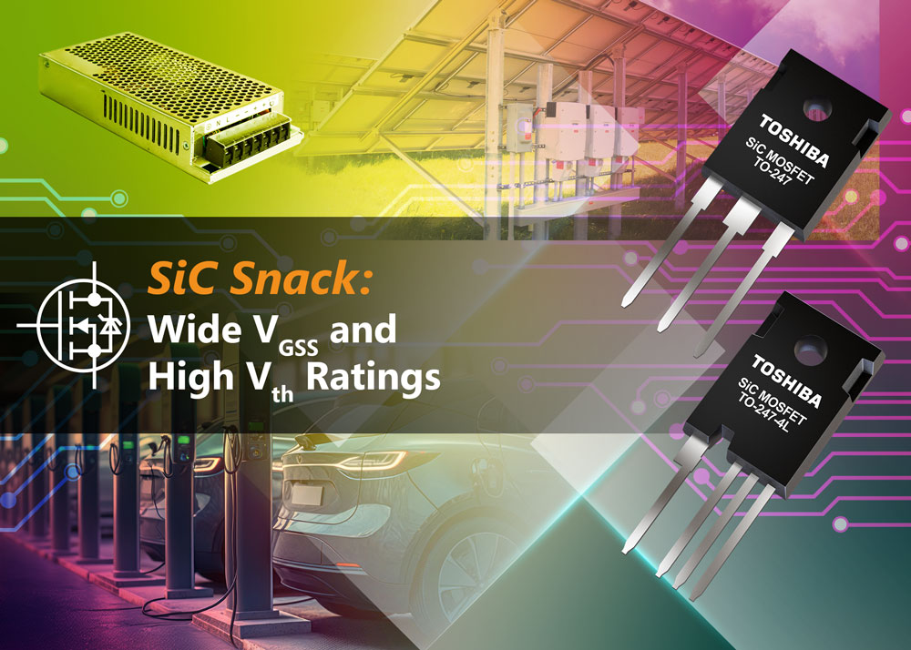
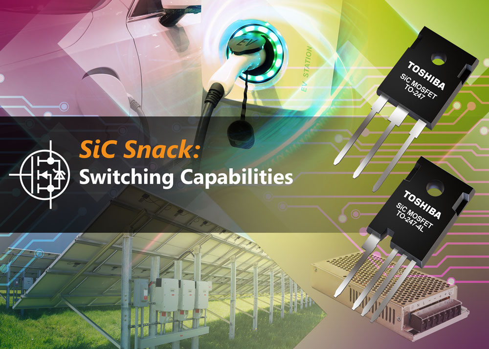
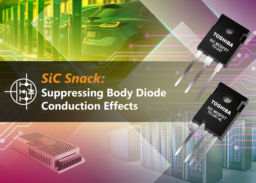
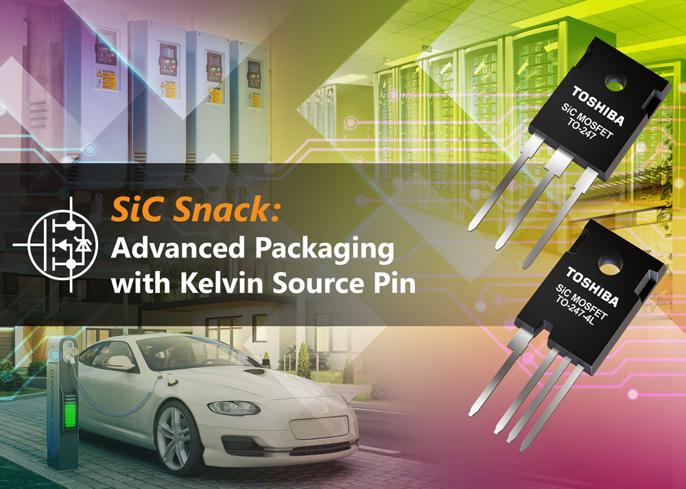
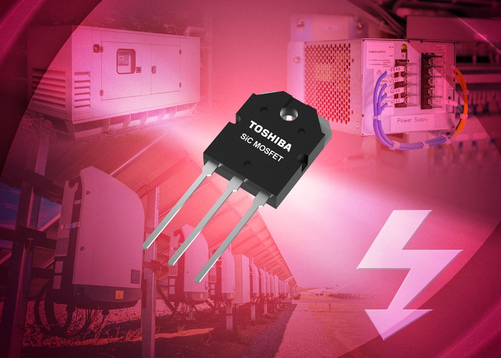
Quickly discover the benefits of Toshiba SiC MOSFETs in bite sized SiC Snacks:
1. Wide VGSS ratings
2. Switching Capabilities
3. The RDS(ON) x Qgd figure of merit (FoM)
4. Suppressing Body Diode Conduction Effects
5. Advanced packaging with Kelvin source pin
Download the snack you're interested in, or download them all together.