
-
My ToshibaSemicon
- 반도체 탑
-
애플리케이션Automotive
Body Electronics
xEV
In-Vehicle Infotainment
Advanced Driver-Assistance Systems (ADAS)
Chassis
IndustrialInfrastructure
BEMS/HEMS
Factory Automation
Commercial Equipment
Consumer/PersonalIoT Equipment
Healthcare
Wearable Device
Mobile
Computer Peripherals
-
제품자동차 디바이스
Discrete Semiconductor
다이오드
트랜지스터
로직 IC
Analog Devices
Digital Devices
Wireless Devices
※
 : Products list (parametric search)파워반도체
※
: Products list (parametric search)Isolators/Solid State RelaysPhotocouplers
Digital Isolators
Solid State Relays
Fiber Optic Transmitting Modules
※
: Products list (parametric search)MOSFETsIGBTs/IEGTs바이폴라 트랜지스터※
: Products list (parametric search)다이오드※
: Products list (parametric search)마이크로컨트롤러모터 드라이버 ICIntelligent Power ICs※
: Products list (parametric search)전원관리IC리니어 IC※
: Products list (parametric search)범용로직IC리니어 이미지 센서기타 제품용 IC기타 제품용 IC
※
: Products list (parametric search) -
개발/설계 지원
-
기술 자료
- 구매처


- 부품 번호 & 키워드 검색
- 상호 참조 검색
- 파라미터 검색
- 재고 확인 및 구매
This webpage doesn't work with Internet Explorer. Please use the latest version of Google Chrome, Microsoft Edge, Mozilla Firefox or Safari.
3글자 이상 입력하세요. Search for multiple part numbers fromhere.
The information presented in this cross reference is based on TOSHIBA's selection criteria and should be treated as a suggestion only. Please carefully review the latest versions of all relevant information on the TOSHIBA products, including without limitation data sheets and validate all operating parameters of the TOSHIBA products to ensure that the suggested TOSHIBA products are truly compatible with your design and application.Please note that this cross reference is based on TOSHIBA's estimate of compatibility with other manufacturers' products, based on other manufacturers' published data, at the time the data was collected.TOSHIBA is not responsible for any incorrect or incomplete information. Information is subject to change at any time without notice.
3글자 이상 입력하세요.
Combinational Logic: Bidirectional Bus Buffers

Bidirectional bus buffers (transceivers)
Example: 74VHC245
A bidirectional bus buffer (transceiver) is a type of logic circuit whose I/O pins can be configured as input and output to receive and transmit data.
Since a transceiver allows the signal direction to be changed via a control signal (DIR), it is used along a bus line through which data are transferred bidirectionally.
The following shows an example of application of a transceiver.
When using bus signals bi-directionally, connect both the bus input and bus output to VCC or GND via a pull-up resistor to prevent the input signal from becoming open (undefined) when the signal is switched by the control signal (DIR).
Please be careful not to short-circuit the output with the output of the bus line when switching signals.
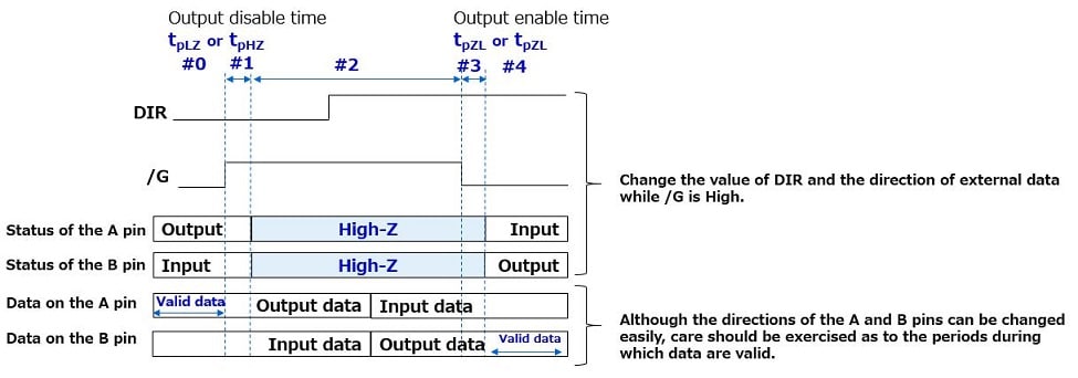
The direction of the A and B pins can be changed easily by changing the value of DIR while /G is High.
Change the value of DIR and the direction of external data while /G is High.
During period #0, data are transferred from B to A.
During period #1, the A pin assumes the High-Z state. Therefore, output data are invalid.
During period #2, change the value of DIR and the direction of external data.
During period #3, enable the A and B pins. Then, output data stabilize at the beginning of period #4.
During period #4, data are transferred from A to B.
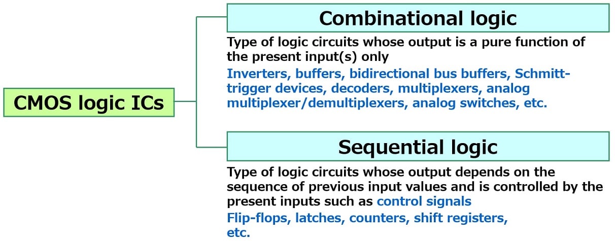
Chapter3 Basic CMOS Logic ICs

Products
Related information
- Application Notes
- FAQ