
-
My ToshibaSemicon
- 반도체 탑
-
애플리케이션Automotive
Body Electronics
xEV
In-Vehicle Infotainment
Advanced Driver-Assistance Systems (ADAS)
Chassis
IndustrialInfrastructure
BEMS/HEMS
Factory Automation
Commercial Equipment
Consumer/PersonalIoT Equipment
Healthcare
Wearable Device
Mobile
Computer Peripherals
-
제품자동차 디바이스
Discrete Semiconductor
다이오드
트랜지스터
로직 IC
Analog Devices
Digital Devices
Wireless Devices
※
 : Products list (parametric search)파워반도체
※
: Products list (parametric search)Isolators/Solid State RelaysPhotocouplers
Digital Isolators
Solid State Relays
Fiber Optic Transmitting Modules
※
: Products list (parametric search)MOSFETsIGBTs/IEGTs바이폴라 트랜지스터※
: Products list (parametric search)다이오드※
: Products list (parametric search)마이크로컨트롤러모터 드라이버 ICIntelligent Power ICs※
: Products list (parametric search)전원관리IC리니어 IC※
: Products list (parametric search)범용로직IC리니어 이미지 센서기타 제품용 IC기타 제품용 IC
※
: Products list (parametric search) -
개발/설계 지원
-
기술 자료
- 구매처


- 부품 번호 & 키워드 검색
- 상호 참조 검색
- 파라미터 검색
- 재고 확인 및 구매
This webpage doesn't work with Internet Explorer. Please use the latest version of Google Chrome, Microsoft Edge, Mozilla Firefox or Safari.
3글자 이상 입력하세요. Search for multiple part numbers fromhere.
The information presented in this cross reference is based on TOSHIBA's selection criteria and should be treated as a suggestion only. Please carefully review the latest versions of all relevant information on the TOSHIBA products, including without limitation data sheets and validate all operating parameters of the TOSHIBA products to ensure that the suggested TOSHIBA products are truly compatible with your design and application.Please note that this cross reference is based on TOSHIBA's estimate of compatibility with other manufacturers' products, based on other manufacturers' published data, at the time the data was collected.TOSHIBA is not responsible for any incorrect or incomplete information. Information is subject to change at any time without notice.
3글자 이상 입력하세요.
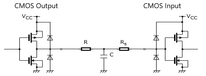
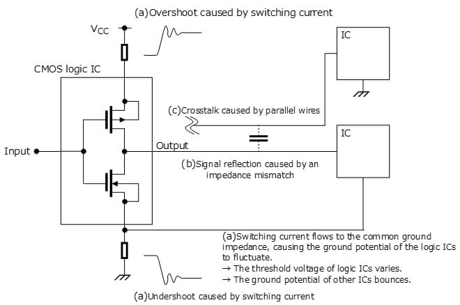
Countermeasures for Signal Reflection
In the case of high-speed CMOS logic ICs, reflections cause an increase in the signal delay, ringing, overshoot, and undershoot. Reflections in transmission lines:
Typical traces have a characteristic impedance(*1) of 50 to 150 Ω. However, the I/O impedance of high-speed CMOS logic ICs differs from the typical characteristic impedance of traces. This impedance mismatch causes part of the transmitted signal to be reflected to both the transmitting and receiving ends of a transmission line.
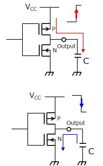
Signal reflection does not affect a slowly rising output because its rise period overlaps that of the reflected signal.
Signal reflection causes a problem when the reflected signal returns to the output after it rises, i.e., when the following equation is true:
tr < 2T
tr: Rise time of the output signal
T: Propagation delay time from the transmitting end to the receiving end of a transmission line
Suppose that the output rise time is 3 ns and that the propagation delay time along a transmission line is 5 ns/m.
Then, signal reflection has a significant impact when the transmission line is 30 cm or longer.
*1 Characteristic impedance
The characteristic impedance is one of the characteristics of a transmission line (e.g., board trace, coaxial cable).
The general expression of the characteristic impedance of a transmission line is Z_0=√(L/C), where L is the inductance per unit length and C is the capacitance per unit length. The unit of characteristic impedance is ohm (Ω). When a termination resistor of 50 Ω is connected to the end of a transmission line with a characteristic impedance of 50 Ω, signal reflection does not occur at the connection point.
However, if the characteristic impedance does not match the resistor value, signal reflection occurs at the connection point.
Countermeasures to reduce Signal Reflection
(1) Increase the board assembly density and reduce the length of board traces to reduce their inductance and capacitance. In this case, however, care is required as to crosstalk between adjacent traces. (See the next page for crosstalk.)
(2) Do not use ICs with an output current higher than necessary.
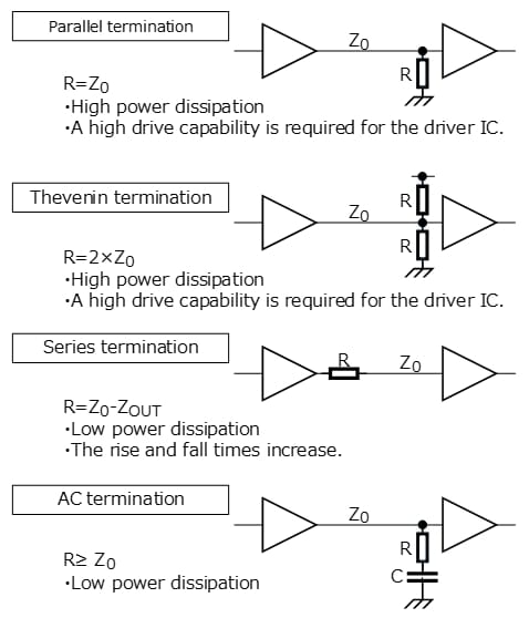
(3) Provide electrical termination so that the I/O impedance of a CMOS logic IC matches the characteristic impedance of the transmission line (See blow figure).
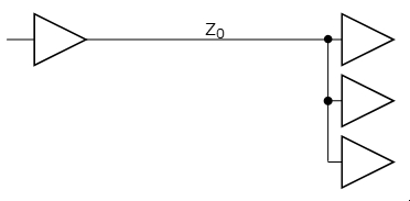
(4) When the output of a CMOS logic IC drives multiple CMOS logic ICs the output trace should be fanned out close to the driven ICs.
Usage Considerations of CMOS Logic ICs


Products
Related information
- Application Notes
- FAQ