
-
My ToshibaSemicon
- 반도체 탑
-
애플리케이션Automotive
Body Electronics
xEV
In-Vehicle Infotainment
Advanced Driver-Assistance Systems (ADAS)
Chassis
IndustrialInfrastructure
BEMS/HEMS
Factory Automation
Commercial Equipment
Consumer/PersonalIoT Equipment
Healthcare
Wearable Device
Mobile
Computer Peripherals
-
제품자동차 디바이스
Discrete Semiconductor
다이오드
트랜지스터
로직 IC
Analog Devices
Digital Devices
Wireless Devices
※
 : Products list (parametric search)파워반도체
※
: Products list (parametric search)Isolators/Solid State RelaysPhotocouplers
Digital Isolators
Solid State Relays
Fiber Optic Transmitting Modules
※
: Products list (parametric search)MOSFETsIGBTs/IEGTs바이폴라 트랜지스터※
: Products list (parametric search)다이오드※
: Products list (parametric search)마이크로컨트롤러모터 드라이버 ICIntelligent Power ICs※
: Products list (parametric search)전원관리IC리니어 IC※
: Products list (parametric search)범용로직IC리니어 이미지 센서기타 제품용 IC기타 제품용 IC
※
: Products list (parametric search) -
개발/설계 지원
-
기술 자료
- 구매처


- 부품 번호 & 키워드 검색
- 상호 참조 검색
- 파라미터 검색
- 재고 확인 및 구매
This webpage doesn't work with Internet Explorer. Please use the latest version of Google Chrome, Microsoft Edge, Mozilla Firefox or Safari.
3글자 이상 입력하세요. Search for multiple part numbers fromhere.
The information presented in this cross reference is based on TOSHIBA's selection criteria and should be treated as a suggestion only. Please carefully review the latest versions of all relevant information on the TOSHIBA products, including without limitation data sheets and validate all operating parameters of the TOSHIBA products to ensure that the suggested TOSHIBA products are truly compatible with your design and application.Please note that this cross reference is based on TOSHIBA's estimate of compatibility with other manufacturers' products, based on other manufacturers' published data, at the time the data was collected.TOSHIBA is not responsible for any incorrect or incomplete information. Information is subject to change at any time without notice.
3글자 이상 입력하세요.
Open a new door for power supply with Toshiba’s SiC MOSFETs
Solving environmental and energy problems is an important global issue. While the demand for electric power continues to escalate, the call for energy conservation and the need for highly efficient and compact electric power conversion systems increases rapidly.
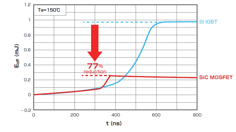
Power MOSFET using new SiC materials offer high voltage resistance, high-speed switching, and low on-resistance properties compared to conventional silicon (Si) MOSFET and IGBT products. This will greatly reduce power dissipation and supports a reduction in the size of equipment.

Introduction to 2nd Generation SiC MOSFETs
Features of 2nd Generation SiC MOSFETs
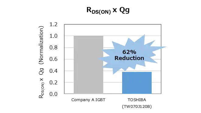
Since the dielectric breakdown strength of SiC (silicon carbide) is about 10 times as high as that of Si (silicon), SiC power devices can offer a high withstand voltages and low voltage drops. The on-resistance per unit area can be reduced in SiC devices compared with that of Si for the same withstand voltage.
What are the merits of using SiC MOSFETs?
Introducing application examples that have improved efficiency by using SiC MOSFETs.
Introduction to Reference Designs with SiC MOSFETs
In the industrial sector, as commoditization and standardization progress, there are increasing cases in which a highly versatile reference design based on device selection and optimal solutions of circuits is used as an efficient development design approach.
This section provides reference designs using SiC MOSFETs for quick advancement of equipment designs.

3-Phase AC 400 V Input PFC Converter
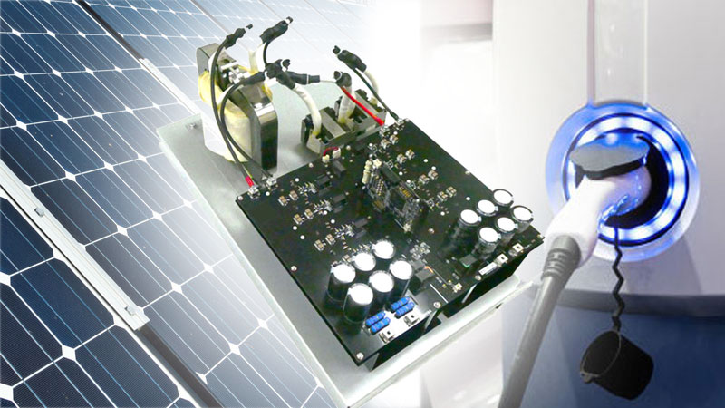
Toshiba's reference design of a power factor correction (PFC) circuit for 3-phase 400 V AC inputs illustrates how to improve power supply efficiency using 2nd Generation SiC MOSFETs. The design achieves a power conversion efficiency of 97% and a power factor of 0.99 or more. It is a reference design for the PFC section (gate drive circuit, sensor circuit, output power switch) of high-power converters such as electric vehicle (EV) charging stations.
The growing adoption of EVs has increased the demand for power conversion systems that must also be highly efficient and compact. This Toshiba reference design provides an excellent starting point for the PFC stage of power converters. It can be used as the basis for both prototyping and developing your application, helping it reach its full potential.
5 kW Isolated Bidirectional DC-DC Converter
The 5kW Isolated Bidirectional DC-DC Converter reference design from Toshiba shows how to improve a power supply design's efficiency using 2nd Generation SiC MOSFETs. The design uses the dual active bridge (DAB) method, one of the most popular topologies for such high-power converters. The DAB topology has full bridges on both sides, allowing the direction and amount of power to be controlled by adjusting the phase difference between the left and right bridge circuits. This highly versatile reference design forms a starting point for developing and prototyping high-power conversion applications, such as electric vehicle charging stations and inverters in solar power generators.