What are the merits of using SiC MOSFETs?
- Efficiency can be improved by replacing power semiconductor components
- What is the power loss using an IGBT?
- What is the power loss replacing with SiC MOSFETs?
- By changing from IGBT to 2nd Generation SiC MOSFETs, power loss is reduced by about 41%.
Product information
| Part Number | Data sheet | Stock Check | Portion Usage | Description |
|---|---|---|---|---|
| TW070J120B | PDF(506KB) |
|
Main switch・6 |
1200 V / 70 mΩ (typ.) @VGS = 20 V / TO-3P(N) |

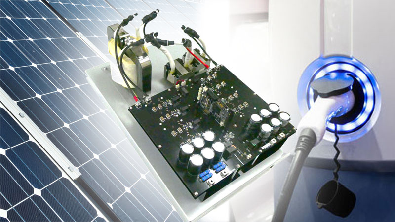
Toshiba Electronic Devices & Storage Corporation provides helpful reference designs relating to its power semiconductors. The company can also provide design support depending on the particular situation. In the following article, an example will be described which shows how efficiency improvements (and consequently power loss reductions) can be enabled via the adoption of 2nd Generation MOSFETs based on silicon-carbide (SiC).
Immediate issue to improve efficiency in existing products
To illustrate the points, let’s look at an actual example. Company A, which is a manufacturer of industrial inverters, had been making efforts to improve efficiency, in response to the market trends already outlined. In addition to new designs, it was necessary to modify the designs and replace the constituent component parts of existing products. Toshiba was called upon to revise the existing version within a short time period. This was done by referring to a relevant reference design.
Company A handles multiple types of inverter products, one of which is a 2kVA output single-phase inverter. This is highly versatile and is widely used in various industrial robots and manufacturing lines. As a result, Customer A’s demands were diverse, with each demand needing to be adequately addressed. In particular, it was necessary to urgently improve efficiency, and existing products were also required to be supported. Therefore, replacement power semiconductor parts needed to be sourced, but with as few changes to the existing design as possible, in order to minimize impact.
Confirmation of target product and loss
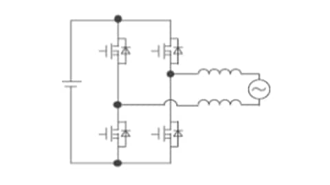
The first attempt to improve efficiency is the 2kVA output single-phase inverter. It was acknowledged that if loss reduction could be achieved, the inverter would be more competitive in the market. However, since this inverter is a low output type and the circuit configuration is simple, there was not much room for efficiency improvement compared to the high output type. Toshiba engineers examined the four IGBTs incorporated into the inverter, and how much loss might be reduced by replacing these switching elements.
Parameter |
Value |
|---|---|
Input voltage |
DC 400V |
Output voltage (effective value) |
AC 200V |
Phase current (effective value) |
10A |
Maximum output |
2kVA |
Switching frequency |
15Hz |
Through communication with Company A, it was confirmed that the loss of the existing model using the IGBT was as follows.
IGBT loss (per element) |
Breakdown |
At phase current 10A: 14.4W |
Conduction loss: 4.4W |
Turn-on switching loss: 3.1W |
|
Turn-off switching loss: 6.9W |
Examination of losses when replacing with SiC MOSFETs
Because the drive conditions of the existing product using IGBTs were such that SiC MOSFETs could also be driven, Toshiba engineers examined the losses when replacement had been undertaken.
1) Conduction losses
Since the current conduction loss of the IGBT was 4.4W, SiC MOSFETs with conduction losses that were basically the same as for the IGBT were considered. The conduction loss could be calculated from the on-resistance of the SiC MOSFETs. The conduction loss in respect to on-resistance and the inverter output phase current was charted (see the graph below). Therefore, SiC MOSFETs with the same conduction loss as existing the IGBTs were considered across a range of potential output phase current conditions.
| On-resistance of SiC MOSFETs |
Conduction loss |
|---|---|
80mΩ |
5.1W |
70mΩ |
4.5W |
60mΩ |
3.9W |
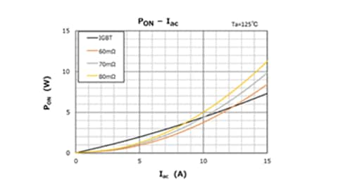
Based on the results obtained, it was decided that the TW070J120B 2nd Generation SiC MOSFETs would be the optimal fit. This device has 70mΩ on-resistance, which translates into almost the same conduction loss (4.4W) as that of the existing IGBT.
2) Switching losses
In the circuit of the existing product, the IGBT was replaced with 2nd Generation SiC MOSFETs TW070J120B. It was calculated that the switching loss at a phase current of 10A, based on the switching waveform and other factors, would lead to turn-on switching loss of 2.5W and a turn-off switching loss of 1.5W.
3) Overall loss comparison
The following is a comparison of each loss between the existing IGBT and the replacement 2nd Generation SiC MOSFETs. By replacing the IGBT with a TW070J120B, the turn-on and turn-off losses were significantly reduced, with a total loss reduction of 5.9W (from 14.4W down to 8.5W) being achieved.
|
Conduction loss |
Turn-on switching loss |
Turn-off switching loss |
Total loss |
|---|---|---|---|---|
IGBT existing model |
4.4W |
3.1W |
6.9W |
14.4W |
Model with TW070J120B replacement |
4.5W (approximately 2% increase) |
2.5W (approximately 19% decrease) |
1.5W (approximately 78% decrease) |
8.5W (approximately 41% decrease) |
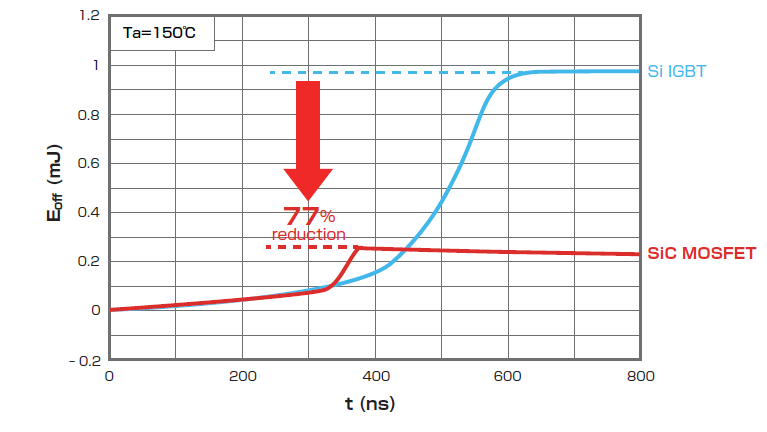
The enhanced switching characteristics of the SiC MOSFETs are largely related to the significant reduction in switching losses. Although IGBTs can achieve high withstand voltage and low on-resistance, they have tail current issues to factor in. In contrast, SiC MOSFETs realize high withstand voltages, low on-resistance and high-speed switching characteristics due to the endemic characteristics of SiC (and its wide bandgap properties). Unlike IGBTs, the device structure does not generate tail current, meaning that switching losses can be kept low.
The following waveform diagram gives a comparison of the switching waveforms of a general IGBT and a TW070J120B 2nd Generation SiC MOSFETs. Although it is not an evaluation waveform in the circuit and operating conditions of this case, it shows the typical characteristics of IC/ID and VCE/VDS at turn-on and turn-off of IGBT and SiC MOSFETs for the gate drive signal under the same conditions. In this example, the IC/ID is 10A and the VCE/VDS is 800V.
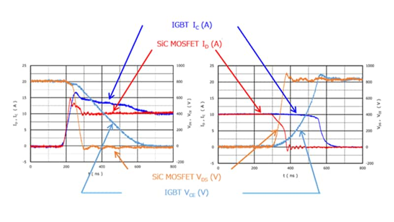

The rise of IC/ID at turn-on is slightly faster for SiC MOSFETs, but the time required for convergence to the set condition of 10A is overwhelmingly faster for SiC MOSFETs. It takes time for the IGBT to converge, with energy being lost during that time. The current that flows during turn-on includes the recovery current of the diode (whether it is external or built-in) between the collector/drain and the emitter/source, so the recovery characteristics of the diode will have an effect.
For the selected TW070J120B SiC MOSFETs, a separate SiC Schottky barrier diode is placed between the drain and source. The recovery characteristics of this diode are high and the recovery current converges quickly. This, combined with high-speed switching, contributes to the reduction of losses during turn-on.
There is a big difference in the IC/ID fall characteristics at turn-off. Since the intrinsic tail current flows through the IGBT, it takes a considerable amount of time to converge to a sufficiently off state. Of course, a large amount of current will flow during that time - resulting in a considerable loss. Since no tail current is generated in the SiC MOSFETs, the loss at turn-off is significantly less.
Ideally, the operation of the switching element turns on and off instantly with respect to the gate signal, with the IC/ID and VCE/VDS immediately converging at the condition value. In other words, any current x voltage (i.e. the electric power) generated other than that is basically a loss. Therefore, the switching characteristics of switching elements are very important for reducing switching loss. It is possible to bring the switching characteristics to a state close to the ideal by optimizing the operating conditions, but it is unavoidable to exclude the basic characteristics, such as the tail current present in IGBTs. If such characteristics prove problematic, the argument for replacing an IGBT with a SiC MOSFETs will have greater validity.
Summary
By changing the switching element of the existing 2kVA single-phase inverter product outlined here, with the IGBT being swapped for a SiC MOSFETs, the loss per element during rated operation was reduced from 14.4W to just 8.5W - which equates to a rate reduction of approximately 41%. This is mainly due to the superior switching capabilities of SiC MOSFETs.
It should be noted that adopting SiC MOSFETs has several advantages other than reducing loss. SiC MOSFETs have excellent operating characteristics in high-temperature environments, and it is possible to simplify heat dissipation measures compared to IGBTs. Furthermore, since the switching losses experienced are so low, it is possible for the system to operate at a higher frequency than an IGBT-based switch could support. If the switching frequency can be increased, the values of the peripheral components (coils and capacitors) can be reduced - thereby enabling space and cost savings to be realized, which could in turn give the product a great competitive edge.
By replacing the IGBT switching elements of Company A's existing products with SiC MOSFETs, Toshiba successfully solved the power loss issues. As well as preparing a reference design that enabled modification of the existing implementation, a great deal of additional support was provided. Toshiba is continuing to develop new technological innovations aimed at improving the performance of SiC MOSFETs, and expanding the lineup of SiC-based power devices offered.
Product information
| Part Number | Data sheet | Stock Check | Portion Usage | Description |
|---|---|---|---|---|
| TW070J120B | PDF(506KB) |
|
Main switch・6 |
1200 V / 70 mΩ (typ.) @VGS = 20 V / TO-3P(N) |