- 半導體首頁
-
應用Automotive
Body Electronics
xEV
In-Vehicle Infotainment
Advanced Driver-Assistance Systems (ADAS)
Chassis
IndustrialInfrastructure
BEMS/HEMS
Factory Automation
Commercial Equipment
Consumer/PersonalIoT Equipment
Healthcare
Wearable Device
Mobile
Computer Peripherals
-
產品車用元件
Discrete Semiconductor
Diodes
電晶體
通用邏輯IC
Analog Devices
Digital Devices
Wireless Devices
※
: Products list (parametric search)
功率半導體※
: Products list (parametric search)
隔離器/固態繼電器Photocouplers
Digital Isolators
※
: Products list (parametric search)
MOSFETsIGBTs/IEGTs雙極性電晶體※
: Products list (parametric search)
Diodes※
: Products list (parametric search)
微控制器馬達驅動 ICs智能功率 ICs※
: Products list (parametric search)
電源管理 ICs線性 ICs※
: Products list (parametric search)
通用邏輯 ICs線性影像感測器其他產品其他產品
※
: Products list (parametric search)
-
開發/設計支援
開發 / 設計支援
-
技術知識
- 購買管道
- 型號 & 關鍵字搜尋
- 交叉搜尋
- 參數搜尋
- 線上庫存查詢跟購買
This webpage doesn't work with Internet Explorer. Please use the latest version of Google Chrome, Microsoft Edge, Mozilla Firefox or Safari.
型號需要超過三個文字以上 Search for multiple part numbers fromhere.
The information presented in this cross reference is based on TOSHIBA's selection criteria and should be treated as a suggestion only. Please carefully review the latest versions of all relevant information on the TOSHIBA products, including without limitation data sheets and validate all operating parameters of the TOSHIBA products to ensure that the suggested TOSHIBA products are truly compatible with your design and application.Please note that this cross reference is based on TOSHIBA's estimate of compatibility with other manufacturers' products, based on other manufacturers' published data, at the time the data was collected.TOSHIBA is not responsible for any incorrect or incomplete information. Information is subject to change at any time without notice.
型號需要超過三個文字以上
使用東芝的SiC MOSFET開啟電源的新大門
解決環境和能源問題是一個重要的全球性問題。隨著電力需求持續升高,對節能的呼聲以及對高效、緊湊型電力轉換系統的需求也迅速增加。
功率半導體具有將直流電轉換成交流電的逆變器功能,將交流電轉換成直流電的轉換器功能,還具有改變交流電頻率的變頻器功能。這些重要器件有助於實現各類產品和不同領域的節能。
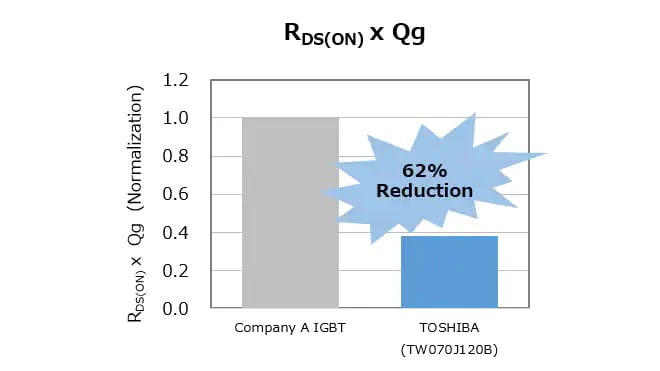
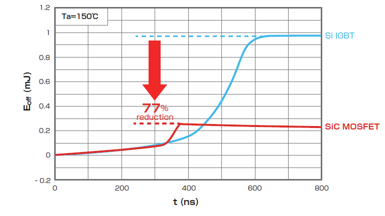
相比于傳統的矽(Si)MOSFET和IGBT產品,基於全新碳化矽(SiC)材料的功率MOSFET具有耐高壓,高速開關,低導通電阻性能。除減少產品尺寸外,該類產品可極大降低功率損耗。

Introduction to 2nd Generation SiC MOSFETs
SiC MOSFET參考設計簡介
隨著工業領域裡商品化和標準化進展,越來越多的案例將基於器件選擇和最優電路解決方案的高度通用參考設計用作有效的開發設計方法。
本章節提供採用SiC MOSFET的參考設計,以便能快速推進您的設備設計進程。

3相AC 400V輸入PFC轉換器
Toshiba's reference design of a power factor correction (PFC) circuit for 3-phase 400 V AC inputs illustrates how to improve power supply efficiency using 2nd Generation SiC MOSFETs. The design achieves a power conversion efficiency of 97% and a power factor of 0.99 or more. It is a reference design for the PFC section (gate drive circuit, sensor circuit, output power switch) of high-power converters such as electric vehicle (EV) charging stations.
The growing adoption of EVs has increased the demand for power conversion systems that must also be highly efficient and compact. This Toshiba reference design provides an excellent starting point for the PFC stage of power converters. It can be used as the basis for both prototyping and developing your application, helping it reach its full potential.

5kW隔離式雙向DC-DC轉換器
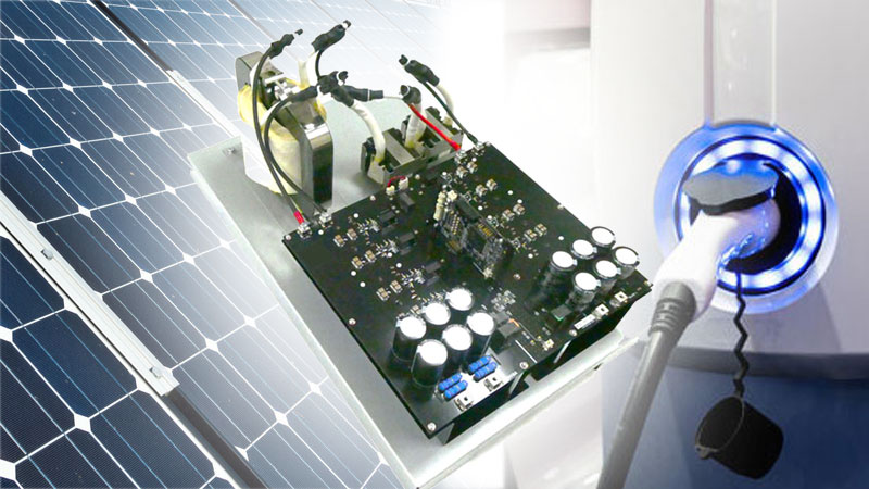
The 5kW Isolated Bidirectional DC-DC Converter reference design from Toshiba shows how to improve a power supply design's efficiency using 2nd Generation SiC MOSFETs. The design uses the dual active bridge (DAB) method, one of the most popular topologies for such high-power converters. The DAB topology has full bridges on both sides, allowing the direction and amount of power to be controlled by adjusting the phase difference between the left and right bridge circuits. This highly versatile reference design forms a starting point for developing and prototyping high-power conversion applications, such as electric vehicle charging stations and inverters in solar power generators.


