
- General Top
- SEMICONDUCTOR
- STORAGE
- COMPANY
-
My ToshibaSemicon
- Semiconductor Top
-
ApplicationsAutomotive
Body Electronics
xEV
In-Vehicle Infotainment
Advanced Driver-Assistance Systems (ADAS)
Chassis
IndustrialInfrastructure
BEMS/HEMS
Factory Automation
Commercial Equipment
Consumer/PersonalIoT Equipment
Healthcare
Wearable Device
Mobile
Computer Peripherals
-
ProductsAutomotive Devices
Discrete Semiconductor
Diodes
Transistors
Logic ICs
Analog Devices
- Automotive SmartMCD™ (Integreted SoC Conbining Microcontroller and Driver)
- Automotive Brushless Motor Driver ICs
- Automotive Brushed DC Motor Driver ICs
- Automotive Stepping Motor Driver ICs
- Automotive Driver ICs
- Automotive System Power Supplies ICs
- Automotive audio power amplifier ICs
- Automotive Network Communication
Digital Devices
Wireless Devices
※
 : Products list (parametric search)Power Semiconductors
SiC Power Devices
※
: Products list (parametric search)Isolators/Solid State RelaysPhotocouplers
Digital Isolators
Solid State Relays
Fiber Optic Transmitting Modules
※
: Products list (parametric search)MOSFETsIGBTs/IEGTsBipolar Transistors※
: Products list (parametric search)Diodes※
: Products list (parametric search)MicrocontrollersMotor Driver ICsIntelligent Power ICs※
: Products list (parametric search)Power Management ICsLinear ICs※
: Products list (parametric search)General Purpose Logic ICsLinear Image SensorsOther Product ICsOther Product ICs
※
: Products list (parametric search) -
Design & Development
Design & Development
Innovation Centre
At the Toshiba Innovation Centre we constantly strive to inspire you with our technologies and solutions. Discover how to place us at the heart of your innovations.
-
Knowledge
Knowledge
Highlighted Topics
Further Materials
Other
- Where To Buy


- Part Number & Keyword Search
- Cross Reference Search
- Parametric Search
- Stock Check & Purchase
This webpage doesn't work with Internet Explorer. Please use the latest version of Google Chrome, Microsoft Edge, Mozilla Firefox or Safari.
require 3 characters or more. Search for multiple part numbers fromhere.
The information presented in this cross reference is based on TOSHIBA's selection criteria and should be treated as a suggestion only. Please carefully review the latest versions of all relevant information on the TOSHIBA products, including without limitation data sheets and validate all operating parameters of the TOSHIBA products to ensure that the suggested TOSHIBA products are truly compatible with your design and application.Please note that this cross reference is based on TOSHIBA's estimate of compatibility with other manufacturers' products, based on other manufacturers' published data, at the time the data was collected.TOSHIBA is not responsible for any incorrect or incomplete information. Information is subject to change at any time without notice.
require 3 characters or more.
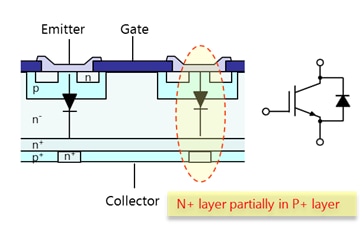
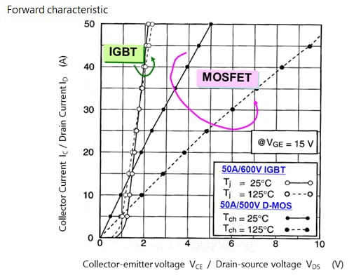
MOSFET Performance Improvement: Decision Factors of RDS(ON)
Download "Chapter III : Transistors" (PDF:2.0MB)
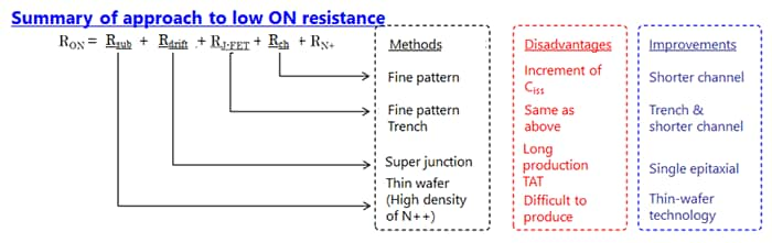
(1) The MOSFET device structure is selected according to the required withstand voltage. The factors that determine the on-resistance RDS (ON) are as shown in Figure 3-7 and Equation 3- (1). Depending on the structure of the device, the ratio of factors determining on-resistance will change.
(2) For example, many middle- and high-voltage MOSFETs (250 V or higher) have planar MOS (π-MOS) structure, and products with less than 200 V have more trench MOS (U-MOS). Therefore, when the withstand voltage VDSS = 600 V, Rdrift becomes the dominant factor, and in the case of 30 V, the ratio of Rch is high.
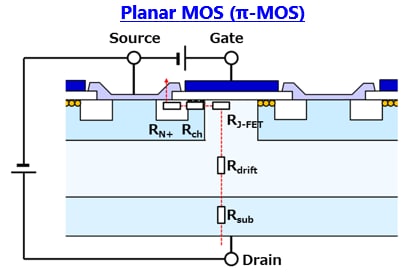
RDS(ON)= Rsub + Rdrift + RJ-FET + Rch + RN+
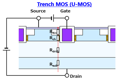
RDS(ON)= Rsub + Rdrift + Rch + RN+ ・・・ Equation 3-(1)
In the case of VDSS=600 V, the order is Rdrift >> Rch > RJ-FET , RN+ , Rsub and RDS(ON) depends on Rdrift
In the case of VDSS=30V, the order is Rch >> Rdrift > RN+ , Rsub. Dependence of RDS(ON) on Rch can be minimized by fine patterning of trench MOS structure.
Chapter III : Transistors


Related information
- Products
- Application Notes
- FAQ