
-
My ToshibaSemicon
- 반도체 탑
-
애플리케이션Automotive
Body Electronics
xEV
In-Vehicle Infotainment
Advanced Driver-Assistance Systems (ADAS)
Chassis
IndustrialInfrastructure
BEMS/HEMS
Factory Automation
Commercial Equipment
Consumer/PersonalIoT Equipment
Healthcare
Wearable Device
Mobile
Computer Peripherals
-
제품자동차 디바이스
Discrete Semiconductor
다이오드
트랜지스터
로직 IC
Analog Devices
Digital Devices
Wireless Devices
※
 : Products list (parametric search)파워반도체
※
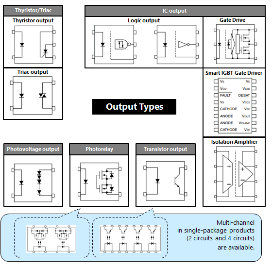
: Products list (parametric search)Isolators/Solid State RelaysPhotocouplers
Digital Isolators
Solid State Relays
Fiber Optic Transmitting Modules
※
: Products list (parametric search)MOSFETsIGBTs/IEGTs바이폴라 트랜지스터※
: Products list (parametric search)다이오드※
: Products list (parametric search)마이크로컨트롤러모터 드라이버 ICIntelligent Power ICs※
: Products list (parametric search)전원관리IC리니어 IC※
: Products list (parametric search)범용로직IC리니어 이미지 센서기타 제품용 IC기타 제품용 IC
※
: Products list (parametric search) -
개발/설계 지원
-
기술 자료
- 구매처


- 부품 번호 & 키워드 검색
- 상호 참조 검색
- 파라미터 검색
- 재고 확인 및 구매
This webpage doesn't work with Internet Explorer. Please use the latest version of Google Chrome, Microsoft Edge, Mozilla Firefox or Safari.
3글자 이상 입력하세요. Search for multiple part numbers fromhere.
The information presented in this cross reference is based on TOSHIBA's selection criteria and should be treated as a suggestion only. Please carefully review the latest versions of all relevant information on the TOSHIBA products, including without limitation data sheets and validate all operating parameters of the TOSHIBA products to ensure that the suggested TOSHIBA products are truly compatible with your design and application.Please note that this cross reference is based on TOSHIBA's estimate of compatibility with other manufacturers' products, based on other manufacturers' published data, at the time the data was collected.TOSHIBA is not responsible for any incorrect or incomplete information. Information is subject to change at any time without notice.
3글자 이상 입력하세요.
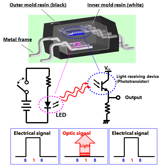
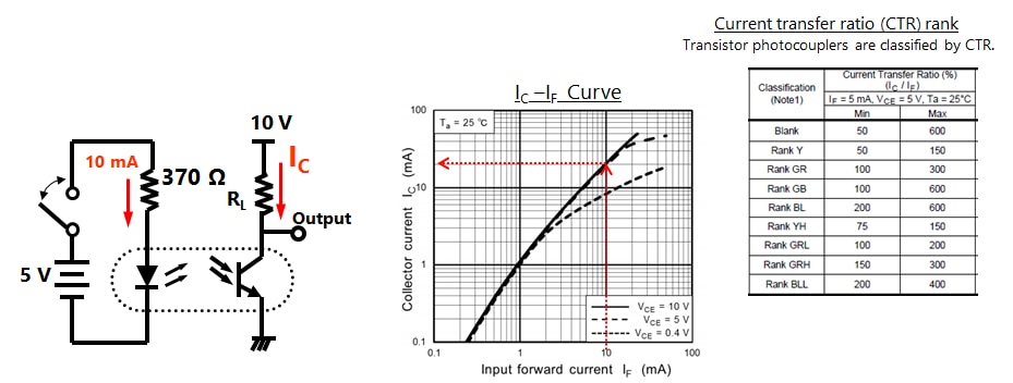
How to Use a Photocoupler “Output-Side Resistor”
Download "Chapter V : Optical Semiconductors" (PDF:1.8MB)
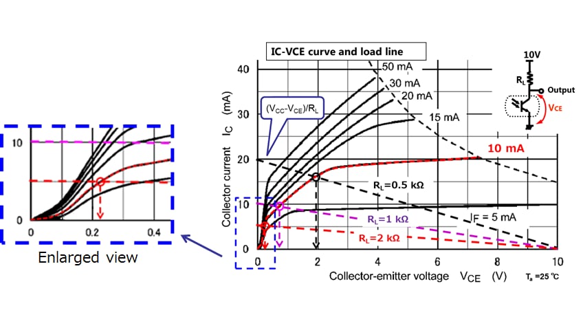
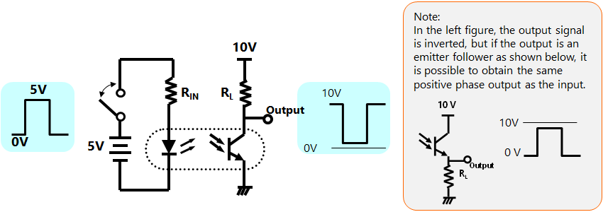
Step 3. Design output-side resistor RL
Determine RL from the IC-VCE characteristics of the output transistor. In order to use for signal transmission, it is necessary to fully satisfy the "L" level of the device connected to the load side.
Here, we set VCE = 0.3 V as the target value.
When IF = 10 mA, VCE = 0.9 V at RL = 1 kΩ, which is insufficient. At RL = 2 kΩ, VCE = about 0.2 V, which satisfies the target value. Therefore, choose RL = 2 kΩ. In actual design, the impedance on the load side must also be considered.
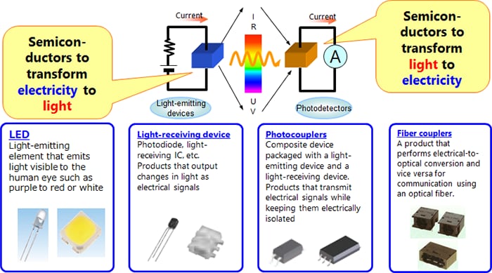
Chapter V : Optical Semiconductors


Related information
- Products
- Application Notes
- FAQ