
- General Top
- SEMICONDUCTOR
- STORAGE
- COMPANY
-
My ToshibaSemicon
- Semiconductor Top
-
ApplicationsAutomotive
Body Electronics
xEV
In-Vehicle Infotainment
Advanced Driver-Assistance Systems (ADAS)
Chassis
IndustrialInfrastructure
BEMS/HEMS
Factory Automation
Commercial Equipment
Consumer/PersonalIoT Equipment
Healthcare
Wearable Device
Mobile
Computer Peripherals
-
ProductsAutomotive Devices
Discrete Semiconductor
Diodes
Transistors
Logic ICs
Analog Devices
Digital Devices
Wireless Devices
※
 : Products list (parametric search)Power Semiconductors
SiC Power Devices
※
: Products list (parametric search)Isolators/Solid State RelaysPhotocouplers
Digital Isolators
Solid State Relays
Fiber Optic Transmitting Modules
※
: Products list (parametric search)MOSFETsIGBTs/IEGTsBipolar Transistors※
: Products list (parametric search)Diodes※
: Products list (parametric search)MicrocontrollersMotor Driver ICsIntelligent Power ICs※
: Products list (parametric search)Power Management ICsLinear ICs※
: Products list (parametric search)General Purpose Logic ICsLinear Image SensorsOther Product ICsOther Product ICs
※
: Products list (parametric search) -
Design & Development
-
Knowledge
- Where To Buy


- Part Number & Keyword Search
- Cross Reference Search
- Parametric Search
- Stock Check & Purchase
This webpage doesn't work with Internet Explorer. Please use the latest version of Google Chrome, Microsoft Edge, Mozilla Firefox or Safari.
require 3 characters or more. Search for multiple part numbers fromhere.
The information presented in this cross reference is based on TOSHIBA's selection criteria and should be treated as a suggestion only. Please carefully review the latest versions of all relevant information on the TOSHIBA products, including without limitation data sheets and validate all operating parameters of the TOSHIBA products to ensure that the suggested TOSHIBA products are truly compatible with your design and application.Please note that this cross reference is based on TOSHIBA's estimate of compatibility with other manufacturers' products, based on other manufacturers' published data, at the time the data was collected.TOSHIBA is not responsible for any incorrect or incomplete information. Information is subject to change at any time without notice.
require 3 characters or more.
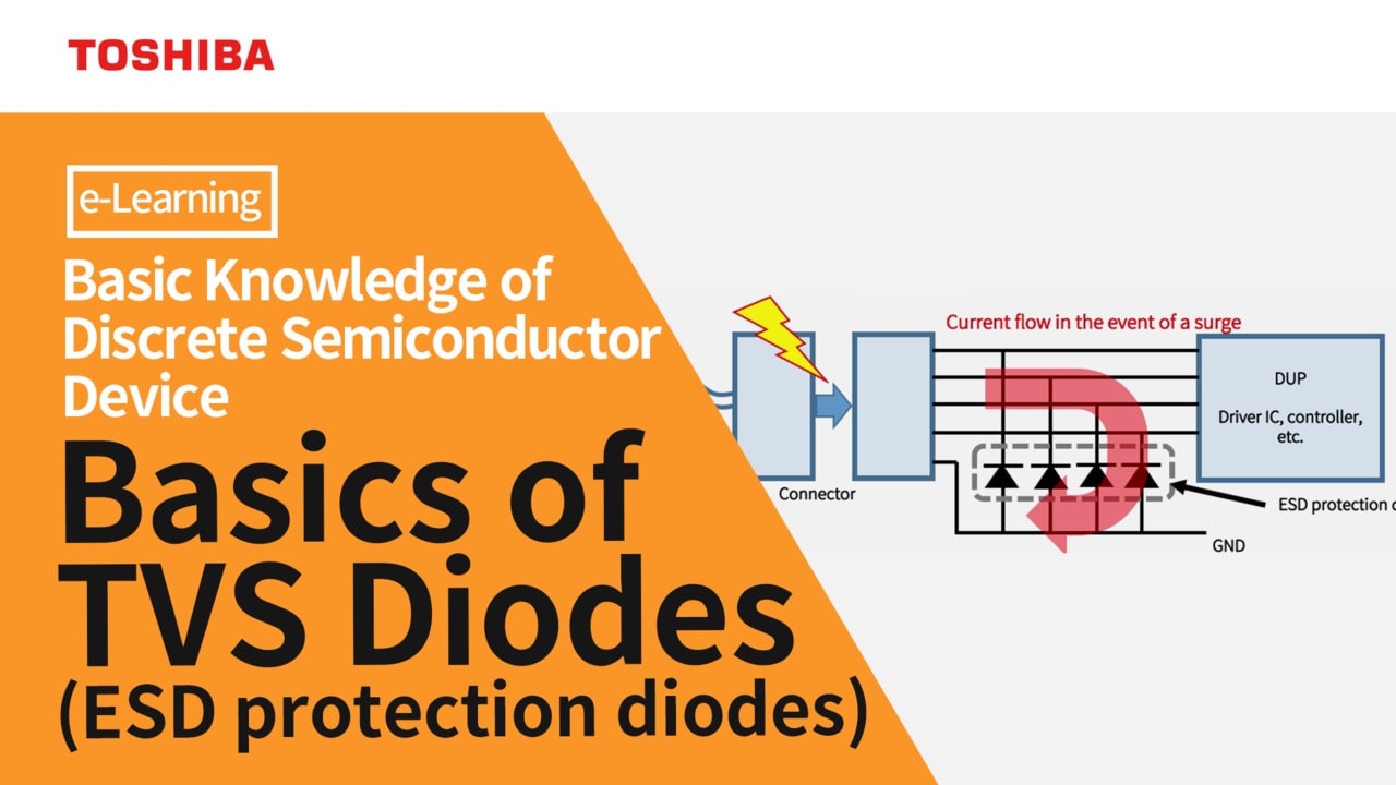
What are the typical electrical characteristics of ESD protection diodes?
The following describes the key electrical characteristics of ESD protection diodes: working peak reverse voltage clamp voltage, dynamic resistance, and working peak reverse voltage. These electrical characteristics are important characteristics that indicate protection performance and other indicators.
Let’s delve into the essential electrical characteristics of ESD protection diodes. These diodes play a crucial role in safeguarding sensitive components, such as integrated circuits (ICs), from harmful electrostatic discharges (ESD). While some of their electrical features resemble those of Zener diodes, ESD protection diodes possess unique properties specifically tailored for their protective function.
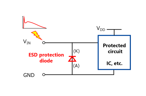
ESD protection diodes do not operate under normal conditions. It turns on only when an abnormal pulse such as ESD enters, safeguarding protected objects such as ICs from unnecessary and harmful energy. Therefore, characteristics from the following perspectives are important.
- Does not turn on under normal conditions (does not distort the passing signal) → Peak reverse operating voltage (VRWM)
- Reliably turns on when an abnormal pulse such as ESD occurs → Clamp voltage (VC)
- Protect the protected element from abnormal pulses → Clamp voltage (VC), dynamic resistance (RDYN)
Each item is explained below.
Working peak reverse voltage VRWM:
Under normal conditions, ESD protection diodes remain inactive and conduct very little current (less than the reverse current IR). VRWM represents the maximum reverse voltage that can be applied without triggering the diode. Exceeding this voltage would cause clamping.
For signal lines, ensure that the maximum voltage (VIN) does not surpass VRWM.
Please also refer to the FAQ below.
How should I select TVS diodes (ESD protection diodes) according to the voltage level of a signal line to be protected?
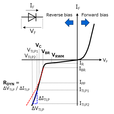
Clamp voltage VC:
This is the on-voltage when high current is applied. Similar characteristics include the reverse breakdown voltage VBR and the Zener voltage VZ of a Zener diode. VBR and VZ are usually defined by small currents (a few mA)
As the name suggests, ESD (Electrostatic Discharge) can be thought of as the discharge of accumulated charge = current. For this reason, clamp voltage is defined as a measure of the voltage value between the anode and cathode (= voltage applied to the protected element) when ESD etc. are applied.
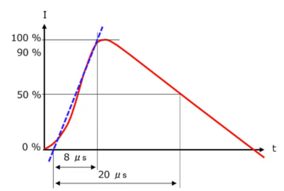
The waveform used for measurement is a current pulse (Fig. 3) specified by IEC61000-4-5. The peak current also varies depending on the product, but it is a high current of 0.5 A to 60 A. The clamp voltage is defined as the maximum voltage between the terminals when this pulse current is applied in the opposite direction of the ESD protection diode.
Regarding IEC61000-4-5, please refer to the FAQ below.
What is IEC61000-4-5?
Reverse breakdown voltage VBR:
This is the rising voltage of the diode in the reverse voltage direction. Although it is sometimes confused with clamp voltage, it is the voltage value when a small current of about 1 mA to 5 mA is passed.
Dynamic resistance RDYN:
This is the slope of the clamp voltage VC at two points with different currents in the reverse voltage direction. VC is generally used as a standard to judge protection performance. Products with lower dynamic resistance can suppress voltage rise at high currents.
For dynamic resistance measurements, two TLP waveforms with different current values are used instead of the IEC6100-4-5 waveform. It is defined below in the same way as general resistance.
RDYN = ΔVTLP / ΔITLP = (VTLP2 – VTLP1) / (ITLP2 – ITLP1)
For products with the same clamp voltage VC, if the dynamic resistance is large, the clamp potential will be high at high current. (Red dotted line in Fig. 1)
Therefore, if the clamp voltage is the same, it can be said that the product with lower dynamic resistance has better protection performance.
Regarding TLP, please refer to the FAQ below.
What is a TLP test?
Related Links
FAQs
Application Notes
The following documents also contain related information.
Company names, product names, and service names used in this FAQ may be of their respective companies.