- General Top
- SEMICONDUCTOR
- STORAGE
- COMPANY
-
My ToshibaSemicon
- Semiconductor Top
-
ApplicationsAutomotive
Body Electronics
xEV
In-Vehicle Infotainment
Advanced Driver-Assistance Systems (ADAS)
Chassis
IndustrialInfrastructure
BEMS/HEMS
Factory Automation
Commercial Equipment
Consumer/PersonalIoT Equipment
Healthcare
Wearable Device
Mobile
Computer Peripherals
-
ProductsAutomotive Devices
Discrete Semiconductor
Diodes
Transistors
Logic ICs
Analog Devices
Digital Devices
Wireless Devices
※
 : Products list (parametric search)Power Semiconductors
SiC Power Devices
※
: Products list (parametric search)Isolators/Solid State RelaysPhotocouplers
Digital Isolators
Solid State Relays
Fiber Optic Transmitting Modules
※
: Products list (parametric search)MOSFETsIGBTs/IEGTsBipolar Transistors※
: Products list (parametric search)Diodes※
: Products list (parametric search)MicrocontrollersMotor Driver ICsIntelligent Power ICs※
: Products list (parametric search)Power Management ICsLinear ICs※
: Products list (parametric search)General Purpose Logic ICsLinear Image SensorsOther Product ICsOther Product ICs
※
: Products list (parametric search) -
Design & Development
-
Knowledge
- Where To Buy


- Part Number & Keyword Search
- Cross Reference Search
- Parametric Search
- Stock Check & Purchase
This webpage doesn't work with Internet Explorer. Please use the latest version of Google Chrome, Microsoft Edge, Mozilla Firefox or Safari.
require 3 characters or more. Search for multiple part numbers fromhere.
The information presented in this cross reference is based on TOSHIBA's selection criteria and should be treated as a suggestion only. Please carefully review the latest versions of all relevant information on the TOSHIBA products, including without limitation data sheets and validate all operating parameters of the TOSHIBA products to ensure that the suggested TOSHIBA products are truly compatible with your design and application.Please note that this cross reference is based on TOSHIBA's estimate of compatibility with other manufacturers' products, based on other manufacturers' published data, at the time the data was collected.TOSHIBA is not responsible for any incorrect or incomplete information. Information is subject to change at any time without notice.
require 3 characters or more.
What are the additional functions (input tolerant, power down protection) required for voltage level conversion and partial power down?
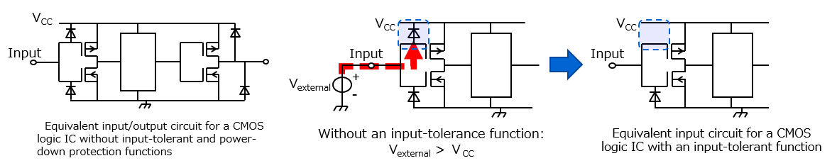
A general logic IC has a diode for protection at the input terminal and the output terminal.
Logic ICs with input tolerant and power down protection functions do not have a diode on the power supply side. This makes it possible to apply a voltage that exceeds the power supply voltage of the logic IC, convert the signal voltage level between ICs operating at different voltages, and partially power down the block connected to the bus system. TOSHIBA calls this function on the input side input tolerant and the output side power down protection.
It is becoming important for CMOS logic ICs, which act as an interface between core ICs and peripheral ICs, to be enhanced with additional functions such as input tolerant function and power down protection.
It is important for CMOS logic ICs, which act as an interface between core ICs and peripheral ICs, to be enhanced with additional functions such as input tolerant functions and power down protection.
Please also refer to the FAQ below.
Level shifting using an input-tolerant function
Input tolerant means that a signal with a level higher than the power supply voltage (VCC) can be input within the operating range when the power is applied or at 0V. By using a product with this function, it is possible to convert the level from high voltage to low voltage.
<Example of voltage level conversion>
5V → 3V voltage conversion: 74VHC or 74LCX is used. 3V → 1.2V voltage conversion: TC74VCX is used.
As shown in the equivalent circuit of a general CMOS logic IC, a diode is intentionally inserted on the input side for the purpose of ESD protection. There is a parasitic diode on the output side. The diode between the input and the power supply may be turned on by applying a voltage of VCC or more of the power supply voltage or applying a voltage when it is off, causing a large current to flow and destroying the element. In such a case, you can prevent the destruction by using a product with an input tolerant function that does not have a diode between the input and the power supply.
Partial power-down is possible if an IC with a power-down protection function is used.
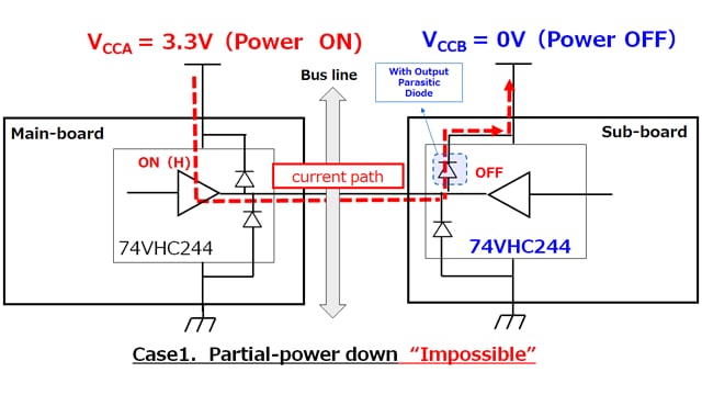
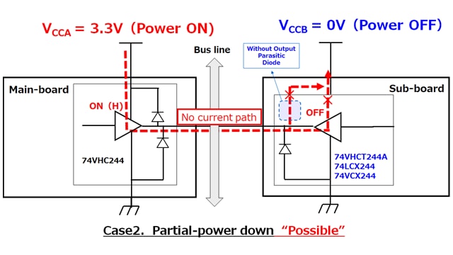
In a system with two power supplies (VCCA, VCCB), there is a case where the VCCB system is shut down (partial power down) in order to reduce power consumption. For example, when the 74VHC series is used for VCCB, there is an unintentional parasitic diode on the output terminal side, so when the condition VCCA> VCCB is satisfied (Case1), the diode between the output and power supply of the system of VCCB turns on. It may cause current to flow and destroy the element. In this case, destruction can be prevented by replacing the product with a product that does not have a parasitic diode at the output in addition to the input (example: 74VHCT series, 74LCX series, 74VCX series). It can be said that these products have power down protection (Case2).