- General Top
- SEMICONDUCTOR
- STORAGE
- COMPANY
-
My ToshibaSemicon
- Semiconductor Top
-
ApplicationsAutomotive
Body Electronics
xEV
In-Vehicle Infotainment
Advanced Driver-Assistance Systems (ADAS)
Chassis
IndustrialInfrastructure
BEMS/HEMS
Factory Automation
Commercial Equipment
Consumer/PersonalIoT Equipment
Healthcare
Wearable Device
Mobile
Computer Peripherals
-
ProductsAutomotive Devices
Discrete Semiconductor
Diodes
Transistors
Logic ICs
Analog Devices
Digital Devices
Wireless Devices
※
: Products list (parametric search)
Power SemiconductorsSiC Power Devices
※
: Products list (parametric search)
Isolators/Solid State RelaysPhotocouplers
Digital Isolators
Solid State Relays
Fiber Optic Transmitting Modules
※
: Products list (parametric search)
MOSFETsIGBTs/IEGTsBipolar Transistors※
: Products list (parametric search)
Diodes※
: Products list (parametric search)
MicrocontrollersMotor Driver ICsIntelligent Power ICs※
: Products list (parametric search)
Power Management ICsLinear ICs※
: Products list (parametric search)
General Purpose Logic ICsLinear Image SensorsOther Product ICsOther Product ICs
※
: Products list (parametric search)
-
Design & Development
-
Knowledge
- Where To Buy
- Part Number & Keyword Search
- Cross Reference Search
- Parametric Search
- Stock Check & Purchase
This webpage doesn't work with Internet Explorer. Please use the latest version of Google Chrome, Microsoft Edge, Mozilla Firefox or Safari.
require 3 characters or more. Search for multiple part numbers fromhere.
The information presented in this cross reference is based on TOSHIBA's selection criteria and should be treated as a suggestion only. Please carefully review the latest versions of all relevant information on the TOSHIBA products, including without limitation data sheets and validate all operating parameters of the TOSHIBA products to ensure that the suggested TOSHIBA products are truly compatible with your design and application.Please note that this cross reference is based on TOSHIBA's estimate of compatibility with other manufacturers' products, based on other manufacturers' published data, at the time the data was collected.TOSHIBA is not responsible for any incorrect or incomplete information. Information is subject to change at any time without notice.
require 3 characters or more.
Improved junction barrier Schottky (JBS) structure to reduce the leakage current and increase the surge current capability: SiC Schottky barrier diodes (SiC SBDs)
While Schottky barrier diodes (SBDs) have advantages such as very short reverse recovery time time (trr) and low forward voltage (VF), they have disadvantages such as high leakage current. Toshiba’s SiC SBDs overcome this drawback through use of an improved structure.
JBS structure to reduce leakage current (IR)
An SBD is formed by the junction of a semiconductor with a metal. It acts as a diode because of a difference in the work function between a semiconductor and a metal. Because the molecular structure may be discontinuous on the semiconductor–metal interface, irregularities on the surface, crystal defects, or other anomalies may occur. Current called leakage current (IR) flows when a high electric field is applied across a semiconductor-metal interface with these defects.
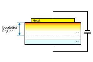
In SBDs with a conventional structure, the depletion region extends into the semiconductor side as shown below, causing the electric field produced by electric charge (or electrons) to be the strongest at the semiconductor-metal interface.
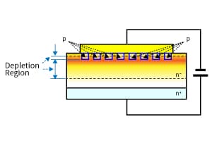
In contrast, in a JBS diode, the depletion region extends between p and n- regions that are partially buried below the semiconductor surface. When the reverse bias voltage increases, p-type depletion regions punch through each other and the position of the maximum electric field moves directly under the p region. This reduces the electric field on the surface where defects may be present thereby reducing leakage current.
Merged PiN Schottky (MPS) structure to increase the surge current capability
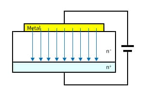
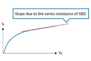
When a conventional SBD is forward-biased, current flows through the following path: metal → Schottky barrier → Si (n-) → Si (n+). The Si (n-) layer has relatively large resistance because of low dopant concentration. Therefore, the IF - VF curve of this SBD looks like the one shown below.
Applications of SiC SBD include PFC circuits, which must be guaranteed to operate at high current because they are instantaneously exposed to large current during the turn-on of a power supply as well as during load variations. In that event, SBDs with an IF - VF curve like the one shown below might be overheated more than expected.
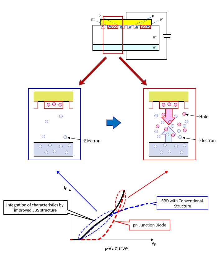
To address this problem, Toshiba has developed new SBDs with an improved JBS structure incorporating the concept of the Merged PiN Schottky (MPS) structure. The MPS structure has p+ regions buried in the n- region of an SBD as shown below. (In Toshiba’s design, part of the p-layer of the JBS structure (the shaded area in the figure) is enlarged and the impurity concentration of this part is increased.) The p+ regions and the n- region form a pn junction diode, which turns on when large current (surge current) is needed. This increases the current-carrying capability of the SBD, thereby reducing a rise in forward voltage even at high current and increasing the maximum allowable surge current value.
The MPS structure is characterized by the p+–n-–n+ configuration below the anode electrode.
At low current, the n- region typically has high resistance. However, when this SBD is forward-biased, holes and electrons flow into the n- region from the p and n regions respectively while maintaining electroneutrality. At this time, both holes and electrons exist in the n- region with high concentration. Consequently, the n- region acts like a heavily doped region, particularly at high current, exhibiting very low resistance (conductivity modulation). As a result, this SBD has an IF-VF curve as shown below, with low VF in the high-current region.
SiC schottky barrier diodes
Related information
Questions about purchasing, sampling and IC reliability
Stock Check & Purchase
require 3 characters or more.

