- General Top
- SEMICONDUCTOR
- STORAGE
- COMPANY
-
My ToshibaSemicon
- Semiconductor Top
-
ApplicationsAutomotive
Body Electronics
xEV
In-Vehicle Infotainment
Advanced Driver-Assistance Systems (ADAS)
Chassis
IndustrialInfrastructure
BEMS/HEMS
Factory Automation
Commercial Equipment
Consumer/PersonalIoT Equipment
Healthcare
Wearable Device
Mobile
Computer Peripherals
-
ProductsAutomotive Devices
Discrete Semiconductor
Diodes
Transistors
Logic ICs
Analog Devices
Digital Devices
Wireless Devices
※
 : Products list (parametric search)Power Semiconductors
SiC Power Devices
※
: Products list (parametric search)Isolators/Solid State RelaysPhotocouplers
Digital Isolators
Solid State Relays
Fiber Optic Transmitting Modules
※
: Products list (parametric search)MOSFETsIGBTs/IEGTsBipolar Transistors※
: Products list (parametric search)Diodes※
: Products list (parametric search)MicrocontrollersMotor Driver ICsIntelligent Power ICs※
: Products list (parametric search)Power Management ICsLinear ICs※
: Products list (parametric search)General Purpose Logic ICsLinear Image SensorsOther Product ICsOther Product ICs
※
: Products list (parametric search) -
Design & Development
-
Knowledge
- Where To Buy


- Part Number & Keyword Search
- Cross Reference Search
- Parametric Search
- Stock Check & Purchase
This webpage doesn't work with Internet Explorer. Please use the latest version of Google Chrome, Microsoft Edge, Mozilla Firefox or Safari.
require 3 characters or more. Search for multiple part numbers fromhere.
The information presented in this cross reference is based on TOSHIBA's selection criteria and should be treated as a suggestion only. Please carefully review the latest versions of all relevant information on the TOSHIBA products, including without limitation data sheets and validate all operating parameters of the TOSHIBA products to ensure that the suggested TOSHIBA products are truly compatible with your design and application.Please note that this cross reference is based on TOSHIBA's estimate of compatibility with other manufacturers' products, based on other manufacturers' published data, at the time the data was collected.TOSHIBA is not responsible for any incorrect or incomplete information. Information is subject to change at any time without notice.
require 3 characters or more.
Contributes to reducing loss of switching power supplies

With the advent of an advanced information society, the amount of information handled every day has dramatically increased, and the increase in power consumed by data centers and information and communications equipment has become a problem on a global scale. Therefore, the demand of high-efficiency for switching power supplies that supply power to data centers and information and communications equipment has been increasing in recent years. Toshiba Electronic Devices & Storage Corporation contributes to higher-efficiency power supplies by developing power MOSFET suitable for switched mode power supplies.
In addition to reducing on-resistance (RDS(ON)), the 80V U-MOSX-H series products that are fabricated with the newest-generation process have improved the product of on-resistance and gate charge (RDS(ON) × Qg)*), the product of on-resistance and gate switch charge (RDS(ON) × QSW)*), and the product of on-resistance and output charge (RDS(ON) × Qoss)*), which are key figures of merit when used in switching applications such as switched mode power supplies, compared to the same voltage products of the previous generation process "U-MOSVIII-H". When a U-MOSX-H is used, the system can be reduced in power dissipation. In addition, the gate threshold voltage (Vth) range is narrowed, and the channel temperature rating (Tch) is increased to 175°C, which contribute to labor-saving and improved flexibility in designs.
* An index for comparing suitability for switching applications by calculating the product of on-resistance and charge quantity characteristics in a trade-off relationship. The smaller this value, the better the performance.
Features
- Optimization of the cell structure by the latest generation process improves the trade-off between on-resistance and charge quantity characteristics
- Low on-resistance characteristics realized by incorporation of the latest generation process and packaging technology
- High rated channel temperature (Tch = 175°C)
- Useful application notes, reference designs, and other documents on the web save design cycle.
Application Notes
Reference Design Center
Key Characteristics
The table below shows the main characteristics of typical products equipped with SOP Advance packaging for U-MOSX-H series products and U-MOSVIII-H series products. With the latest processing techniques, U-MOSX-H Series offers a significant reduction in drain-to-source on-resistance. U-MOSX-H series products contribute to the reduction of equipment loss caused by on-resistance or the reduction of board area by reducing the number of mounted elements.
U-MOSX-H Series and U-MOSVIII-H Series Product Key Characteristics
|
Characteristics |
U-MOSX-H Series |
U-MOSVIII-H Series |
|
|---|---|---|---|---|
Absolute maximum ratings |
Drain-source voltage VDSS(V) |
80 |
80 |
|
Channel temperature Tch(℃) |
175 |
150 |
||
Electrical characteristics |
Gate threshold voltage Vth(V) |
@VDS = 10V, |
2.5 to 3.5 |
2.0 to 4.0 |
Drain-source on-resistance RDS(ON) typ(mΩ) |
@VGS = 10V |
1.9 |
3.3 |
|
Total gate charge Qg typ(nC) |
87 |
59 |
||
Gate switch charge QSW typ(nC) |
28 |
18 |
||
Output charge Qoss typ(nC) |
90 |
77 |
||
Input capacitance Ciss typ(pF) |
5870 |
4100 |
||
Switching figure of merit
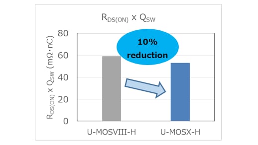
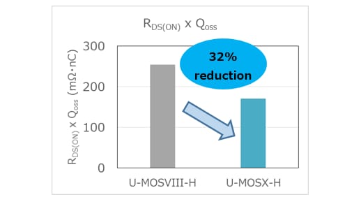
U-MOSX-H series dramatically improves (reduces) RDS(ON)×Qg, RDS(ON)×QSW and RDS(ON)×QOSS, which are key performance indexes for MOSFET, by optimizing cell structures using the latest fine-pitched techniques. The figures below compare the performance indices of U-MOSX-H and U-MOSVIII-H series. These improvements in the figure of merit reduce the major losses such as conduction loss, drive loss, switching loss, and output charge loss, and contribute to higher efficiency in power supply equipment and lower device temperatures.

RDS(ON) : On-resistance (figure of merit for conduction loss)
Qg : Gate charge (figure of merit for drive loss)
QSW : Gate switch charge (figure of merit for switching loss)
QOSS : Output charge (figure of merit for output charge loss)
Recommended Product List
Part Number |
TPH2R408QM |
TPN19008QM |
||
|---|---|---|---|---|
Datasheet |
||||
Package (Width×Length×Height mm) |
SOP Advance (N)  |
TSON Advance
|
||
Absolute Maximum Ratings |
Drain-source voltage VDSS(V) |
80 |
80 |
|
Channel temperature Tch(℃) |
175 |
175 |
||
Electrical Characteristics |
Gate threshold voltage Vth(V) |
@VDS = 10V, |
2.5 to 3.5 |
2.5 to 3.5 |
Drain-source on-resistance RDS(ON) typ(mΩ) |
@VGS = 10V |
1.9 |
14.7 |
|
Total gate charge Qg typ(nC) |
87 |
16 |
||
Gate switch charge QSW typ(nC) |
28 |
5.5 |
||
Output charge Qoss typ(nC) |
90 |
16.5 |
||
Input capacitance Ciss typ(pF) |
5870 |
1020 |
||