
- General Top
- SEMICONDUCTOR
- STORAGE
- COMPANY
-
My ToshibaSemicon
- Semiconductor Top
-
ApplicationsAutomotive
Body Electronics
xEV
In-Vehicle Infotainment
Advanced Driver-Assistance Systems (ADAS)
Chassis
IndustrialInfrastructure
BEMS/HEMS
Factory Automation
Commercial Equipment
Consumer/PersonalIoT Equipment
Healthcare
Wearable Device
Mobile
Computer Peripherals
-
ProductsAutomotive Devices
Discrete Semiconductor
Diodes
Transistors
Logic ICs
Analog Devices
Digital Devices
Wireless Devices
※
 : Products list (parametric search)Power Semiconductors
SiC Power Devices
※
: Products list (parametric search)Isolators/Solid State RelaysPhotocouplers
Digital Isolators
Solid State Relays
Fiber Optic Transmitting Modules
※
: Products list (parametric search)MOSFETsIGBTs/IEGTsBipolar Transistors※
: Products list (parametric search)Diodes※
: Products list (parametric search)MicrocontrollersMotor Driver ICsIntelligent Power ICs※
: Products list (parametric search)Power Management ICsLinear ICs※
: Products list (parametric search)General Purpose Logic ICsLinear Image SensorsOther Product ICsOther Product ICs
※
: Products list (parametric search) -
Design & Development
-
Knowledge
- Where To Buy


- Part Number & Keyword Search
- Cross Reference Search
- Parametric Search
- Stock Check & Purchase
This webpage doesn't work with Internet Explorer. Please use the latest version of Google Chrome, Microsoft Edge, Mozilla Firefox or Safari.
require 3 characters or more. Search for multiple part numbers fromhere.
The information presented in this cross reference is based on TOSHIBA's selection criteria and should be treated as a suggestion only. Please carefully review the latest versions of all relevant information on the TOSHIBA products, including without limitation data sheets and validate all operating parameters of the TOSHIBA products to ensure that the suggested TOSHIBA products are truly compatible with your design and application.Please note that this cross reference is based on TOSHIBA's estimate of compatibility with other manufacturers' products, based on other manufacturers' published data, at the time the data was collected.TOSHIBA is not responsible for any incorrect or incomplete information. Information is subject to change at any time without notice.
require 3 characters or more.
U-MOS X-H series 150 V MOSFET ideal for efficient switching power supplies
Toshiba Electronic Devices & Storage Corporation has developed U-MOS X-H 150 V process power MOSFET (metal-oxide-semiconductor field-effect transistor) series with dramatically improved on-resistance and charge characteristics for switching power supplies that require high-efficiency, such as power supplies for telecommunication base stations and power supplies for datacenter servers. It contributes to improvement of additional value such as efficiency improvement, compactness, and cost reduction of power supplies.
Expansion of 150 V MOSFET applications

High-capacity contents that require high-rate communication such as video streaming is increasing and 5G (5th-generation mobile communications system) services which meet the high-rate communication was launched. Therefore, telecommunication base stations and datacenter servers become more and more and power supplies of those require high efficiency.
At the base stations, AC (alternating current) to DC (direct current) converters convert commercial AC voltage to DC -48 V which is common voltage of telecommunication power supplies, and then DC to DC converters convert the DC -48 V to an appropriate voltage which requires high frequency amplifiers or system control.
48 V power supplies become popular in datacenter servers that capacity is increasing, to reduce power loss of voltage bus.
High-performance MOSFETs are essential for switching power supplies for telecommunication base stations and datacenter servers that require high-efficiency and improving device performance become more important day by day.
Features of U-MOS X-H Series 150 V MOSFET
- Improved trade-off between on-resistance and charge characteristics by device structure optimization and fine process technology
- Reduced reverse recovery loss and spike voltage by built-in high-speed diode (HSD) with lifetime control technology
- High temperature operation capability by high channel temperature rating (Tch = 175 °C)
- Available useful contents which help efficient design such as application notes, reference designs and so on
It is necessary to reduce conduction loss when switching device is ON and switching loss during the device turn ON/OFF in order to improve efficiency of power supplies. In the MOSFET case, it is essential to improve certain characteristics such as on-resistance (RDS(ON)), gate-switch charge (Qsw), output charge (Qoss), and reverse-recovery charge (Qrr).
In general, cell pitch is fined to improve RDS(ON) value, but Qg, Qoss, and Qrr values become bigger by fining the cell pitch only. Therefore, following FOM (figure of merit) need to be reduced, product of the on-resistor and the gate-switch charge (RDS(ON)・Qsw), product of the on-resistor and the output charge (RDS(ON)・Qoss), and product of the on-resistor and the reverse-recovery charge (RDS(ON)・Qrr).
Aiming to reduce the both conduction loss and switching loss, the U-MOSX-H series 150 V MOSFET achieves 38 % reduction of RDS(ON), 12 % reduction of Ron・Qsw and 57 % reduction of Ron・Qrr* due to the device structure optimization and fine process technology based on conventional generation device structure.
(*Standard (STD) product case, compared to conventional generation U-MOSVIII-H)
Products with internal high-speed diode (HSD) which can reduce reverse recovery loss and spike voltage that life-time control technology applies to are also added into the product lineup. Furthermore, the HSD type products reduce 74 % of Ron・Qrr compared with the STD type products.
U-MOS X-H products also support high temperature operation up to 175 °C. (Up to 150 °C for conventional generation U-MOSVIII-H products)
The mentioned above contributes to improvement of additional value such as efficiency improvement, compactness, and cost reduction of power supplies.
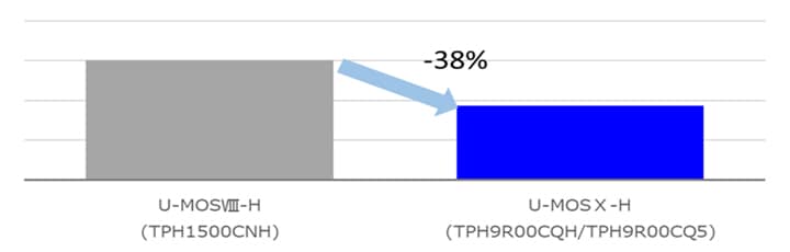
On-resistance (RDS(ON))
In U-MOS X-H series 150 V MOSFET, the on-resistance has been reduced by 38 % compared with the conventional U-MOSVIII-H series 150 V MOSFET by using the most advanced fine pitch process technology. This reduces conduction loss and improves efficiency then reducing the number of devices connected in parallel, reducing costs by reducing the mounting area, and reducing the size of the power supply become possible.
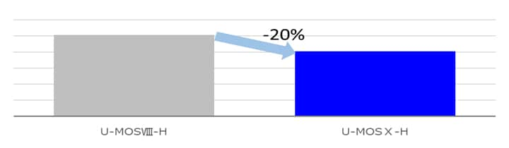
Output Charge (Qoss)
In a switching circuit, the output capacitance (Coss) is charged at every turn off and the charged charge (Qoss) becomes power loss without any use. This makes a part of the switching loss. The U-MOS X-H series 150 V MOSFET reduce 20 % of Qoss compared with U-MOSVIII-H series 150 V MOSFET in the case of same on-resistance devices.
Reverse recovery charge (Qrr)
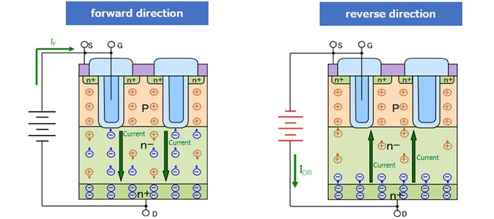
In a synchronous rectifier circuit, an operation which the biased direction of built-in diode is steeply reversed from a state which current flow through the built-in diode in the forward direction occurs. At this time, the reverse current (IDR) continues to flow thorough the built-in diode during the time that accumulated carriers (holes and electrons) in n-semiconductor are extinguished by discharge or recombination (trr: reverse recovery time). The loss due to this reverse recovery charge (Qrr) is called reverse recovery loss.
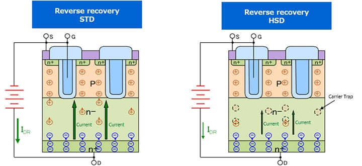
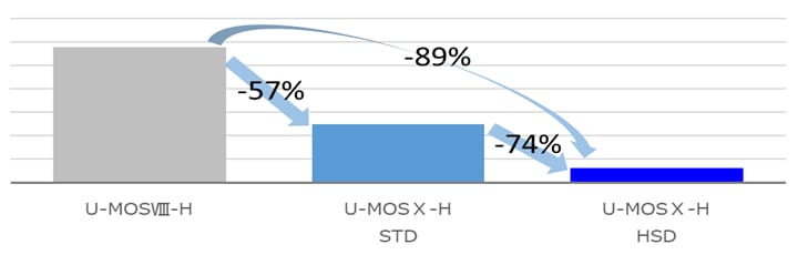
In U-MOS X-H series 150 V MOSFET, the Qrr has been reduced by 57 % compared with the conventional U-MOSVIII-H series 150 V MOSFET in the case of same on-resistance devices. However, if a lower on-resistance device is used or multiple devices are used in parallel when applications need low on-resistance characteristics, the proportion of reverse recovery loss due to Qrr to the total power loss will be larger than the proportion of conduction loss to the total power loss. Then, we have additionally launched the high-speed diode (HSD) type products which the carrier trap to reduce mobility of carrier by the recombination of carrier applies to, in order to reduce Qrr more. Products which this process does not apply to are as the standard products (STD) and the following figure shows the difference of reverse recovery behavior between the HSD and STD. The Qrr value of U-MOSX-H series HSD product is 74 % reduced compared with the U-MOSX-H series STD products and is 89 % reduced compared with the U-MOSVIII-H series products in the case of same on-resistance devices.
Follow the links below for U-MOS X-H series 150 V MOSFET
Related link
Follow the links below for reference design information using 150 V MOSFET
1 kW Non-Isolated Buck-Boost DC-DC Converter for Telecommunication Equipment
3-Phase Multi-Level Inverter using MOSFET
1 kW Full-Bridge DC-DC Converter
Follow the links below for application information using 150 V MOSFET
Server
Inverter/Servo
Follow the links below for electrical models for circuit simulation, PSpice®, LTspice®, etc
High accurate models
MOSFET SPICE model grade (2.21MB)
Switched Mode Power Supply Library
Online Circuit Simulator